
We have a guest contribution today from Israel Beinglass, MonolithIC 3D Inc.'s CTO. Israel talks about how 3D technology can accelerate Moore's Law by providing more than 2x transistor density every two years.
Is it possible to actually accelerate Moore’s law? Sounds like a bad joke? Let’s walk together through some of Moore’s Law's history and cost issues. At the end I’ll try to show you that it is possible.
Gordon Moore in his April 19 1965 article titled “Cramming more components onto integrated Circuits” discussed the following which later became Moore’s Law, Electronic, 38, 8, April 19 1965
1.…… "scientific advances affecting semiconductors could be crucial to economic growth, because an extensive range of applications would be found for more powerful devices in industry, government and national defense"
2.…… "it would depend on a tradeoff between the pace of scientific advance and the costs of producing more powerful devices"
3.…….“Integrated circuits will lead to such wonders as home computers – or at least terminals connected to a central computer – automatic controls for automobiles, and personal portable communications equipment. The electronic wristwatch needs only a display to be feasible today.”
4. … “the biggest potential lies in the production of large systems. In telephone communications, integrated circuits in digital filters will separate channels on multiplex equipment. Integrated circuits will also switch telephone circuits, and perform data processing” See Figure1.
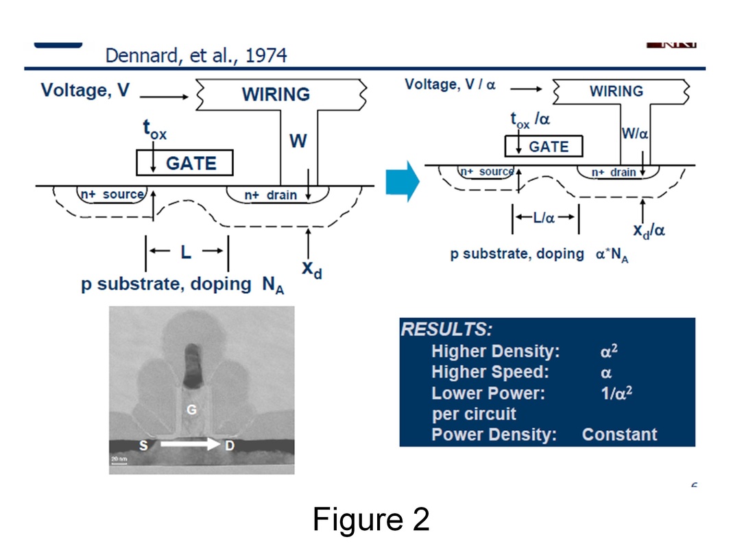
Later on, this discussion became the famous “Moore’s Law”. We can’t ignore the complementary Dennard contribution – the scaling idea (Figure 2). Without its implementation over the years, the semiconductor world would not be the way it has been. IEEE J. of Solid State Physics Oct 1974, 256-267.
Gordon Moore in his April 19 1965 article titled “Cramming more components onto integrated Circuits” discussed the following which later became Moore’s Law, Electronic, 38, 8, April 19 1965
1.…… "scientific advances affecting semiconductors could be crucial to economic growth, because an extensive range of applications would be found for more powerful devices in industry, government and national defense"
2.…… "it would depend on a tradeoff between the pace of scientific advance and the costs of producing more powerful devices"
3.…….“Integrated circuits will lead to such wonders as home computers – or at least terminals connected to a central computer – automatic controls for automobiles, and personal portable communications equipment. The electronic wristwatch needs only a display to be feasible today.”
4. … “the biggest potential lies in the production of large systems. In telephone communications, integrated circuits in digital filters will separate channels on multiplex equipment. Integrated circuits will also switch telephone circuits, and perform data processing” See Figure1.
Later on, this discussion became the famous “Moore’s Law”. We can’t ignore the complementary Dennard contribution – the scaling idea (Figure 2). Without its implementation over the years, the semiconductor world would not be the way it has been. IEEE J. of Solid State Physics Oct 1974, 256-267.

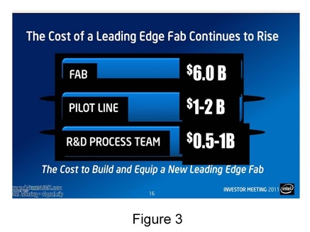
Let’s review some macro semiconductor data relating to the issues discussed above. Figure 3 is a summary of costs associated with a new Fab. Obviously these expenses are incredibly high which caused many small and medium (even some big) companies to drop out of building their own chips and rely on the foundry business model that in turn has been flourishing for the last decade. There are about 1000 Fabless companies around the globe, reinforcing the foundry model!!!
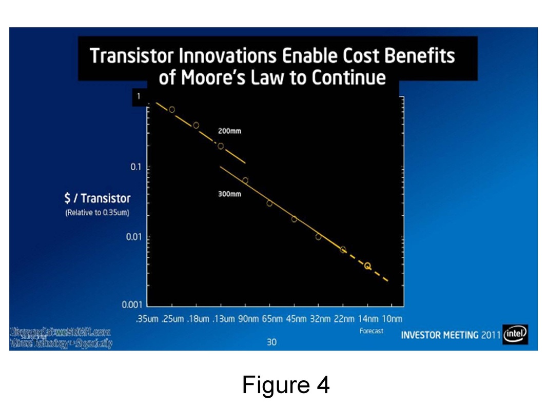
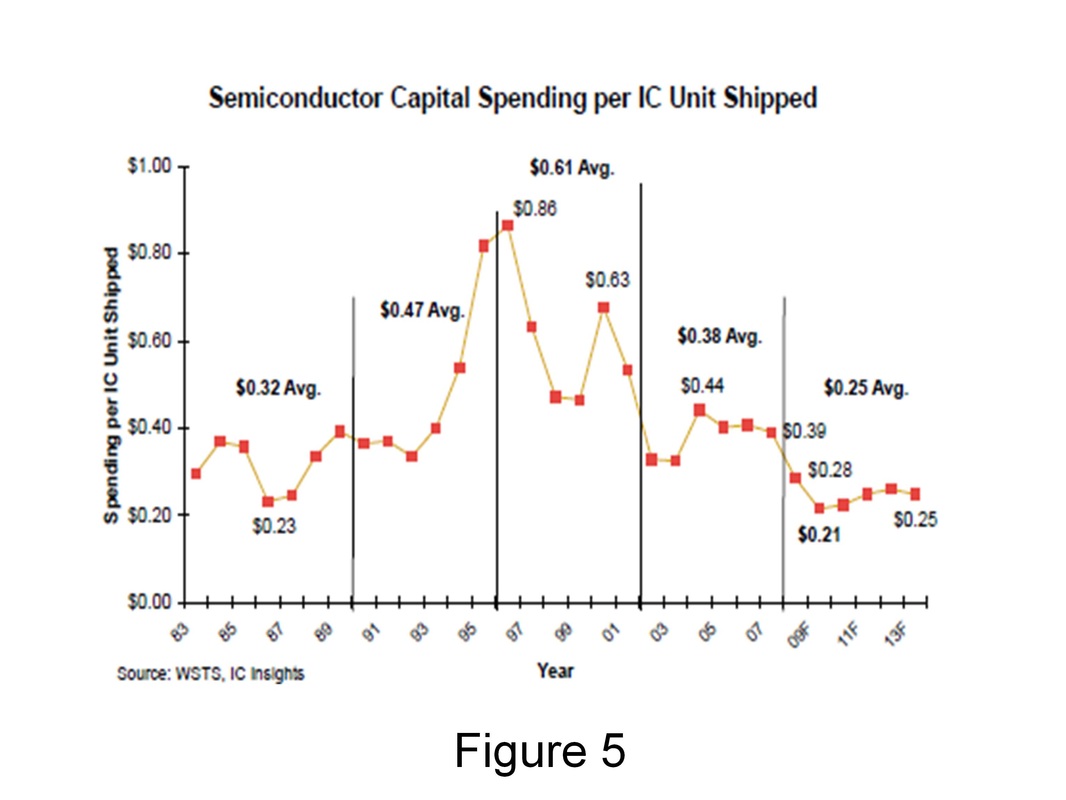
Even with the high costs of new Fabs, some large IDMs as well as memory manufacturers are still continuing to build Fabs to manufacture chips. Figure 4 shows that continuing Moore’s law and increasing wafer size actually lowers the cost of the individual transistor (thanks to scaling). Figure 5 shows the trend of Semiconductor Capital spending per IC unit shipped also trends down. The equipment companies, though charging a lot for their products have increased throughput over the years to some very impressive numbers. Throughput of the most advanced Immersion Steppers is way above 100wafers/hour as well as some of the medium current implant can achieve more than 200wafers/Hr. All these reinforce the fact that Moore’s law is still alive (at least for now) and the main issue is really the cost of an individual new advanced Fab.
So, at this point, Moore’s law has the potential to continue to smaller nodes for manufacturers such as Intel and others who can afford to build $6B fabs. For these manufacturers, the obvious next step to accelerate Moore’s law is to combine smaller feature sizes with the Monolithic 3D concept by building 2 (or more) scaled devices one on top of the other. By doing this we are increasing the density of the 2 chips by 2x, hence we are advancing Moore’s law and accelerating density and number of transistors!!!


 RSS Feed