
We have a guest contribution today from Israel Beinglass, the CTO of MonolithIC 3D Inc. Israel discusses the opportunities of 3D NAND with Monolithic 3D.
NAND technology, which is a subset of NVM (Non Volatile Memory), was invented by Fujio Masuoka of Toshiba back in 1984. Flash memory was presented at IEDM1984 by Dr. Masuoka and his colleagues [1]. The following is a short quote from the original paper “the cell is programmed by a channel hot carrier injection mechanism similar to EPROM. The contents of all memory cells are simultaneously erased by using field emission of electrons from a floating gate to an erased gate in a FLASH (Hence the name FLASH)â€.
Masuoka came back to the IEDM in 1987 and suggested a Flash NAND structure [2].
Intel created the first commercial NOR type of Flash chips in 1988. For the next few years some major developments occur in the Flash arena:
Masuoka came back to the IEDM in 1987 and suggested a Flash NAND structure [2].
Intel created the first commercial NOR type of Flash chips in 1988. For the next few years some major developments occur in the Flash arena:
- In 1989, Samsung and Toshiba created a NAND flash memory.
- In 1994, Compact Flash was invented and introduced by SanDisk.
- In 1999, the SD memory card was released by a combination of SanDisk, Toshiba and Matsushita.
- In 2001, the world’s first 1 Gigabit Compact Flash card was introduced.
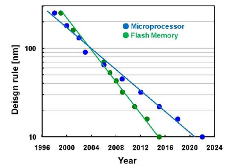
Figure 1: Flash Vs. Microprocessor design rules cross over
NAND memory as a true cross point array with the control gate on top of the floating gate and only one contact for a whole string of cells has the smallest memory cell size as shown in Figure 2 In addition, when one adds with the capability of MLC (Multi Level Cells) to NAND devices, the bit density dramatically increases.
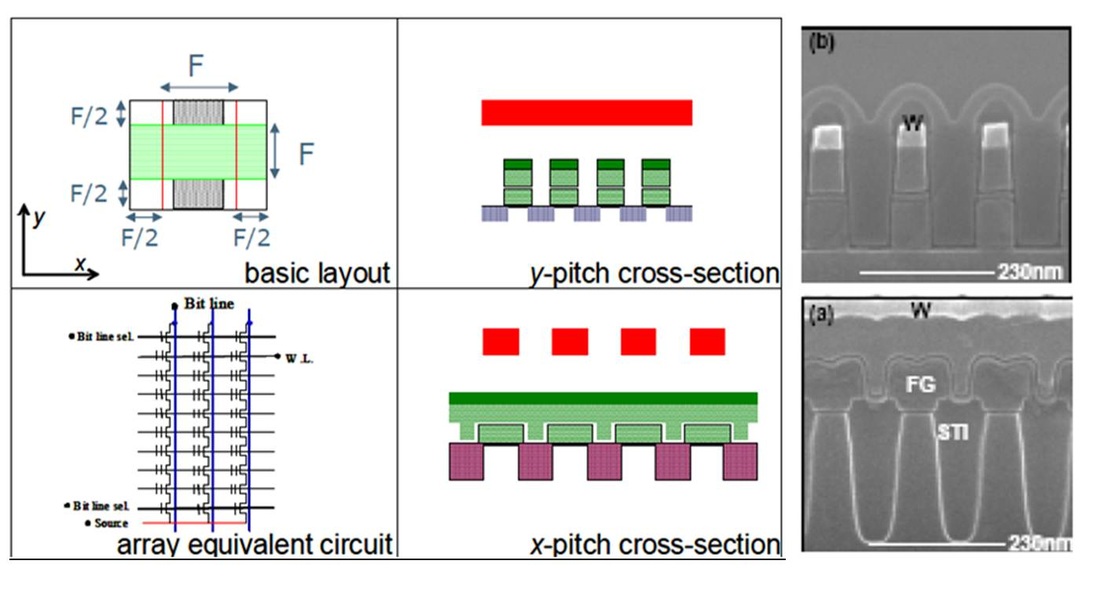
Figure 2: NAND, circuit diagram and SEM pictures in x and y directions.
The NAND market has been continuously growing for the last several years. Figure 3 shows the NAND revenue and Gigabytes increase since 2008 and the forward projection for the years 2012-2016.
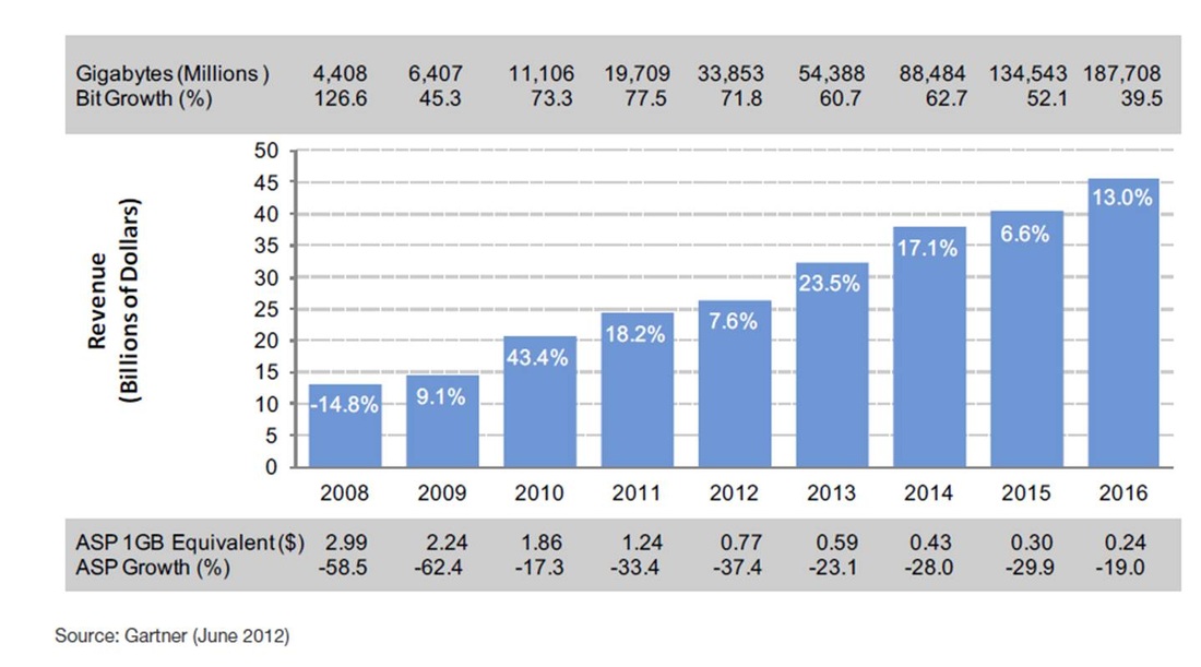
Figure 3: NAND Revenue and Gigabytes growth
As the NAND technology has been moving to smaller and smaller process nodes some serious problems, physical and electrical surfaced:
Physical Limitations:
Physical Limitations:
- Pattern scaling - lack of EUV is a major issue
- Structure formation, Figure 4 depicts a 27nm NAND cell that shows how close the cells are getting to each other, and how much the aspect ratio is getting out of hand. This is a limiter to obtaining high yield.
- There is an increase in cell-to-cell interference in the word lines.
- Capacitive coupling ratio has decreased
- Dielectric leakage has increased
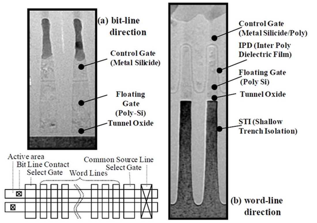
Figure 4: A 27nm NAND cell structure

Figure 5: Number of electrons on the FG decreases for advanced NAND technology nodes
It is a common understanding among the experts that the current NAND technology will not be able to be scaled down to the 10nm node.
The solution for this dilemma is the 3D NAND, which was initially proposed by Toshiba at the 2007 VLSI Symposium [3]. Toshiba unveiled its Bit Cost Scalable (BiCS) technology. BiCS makes use of a “punch-and plug†structure and charge trap memory films. Toshiba has fabricated a prototype 32-Gbit BiCS flash memory test array with a 16-layer memory cell using 60nm design rules, see Figure 6. Hynix, Samsung and Macronix have also come with their versions of the 3D NAND.
The solution for this dilemma is the 3D NAND, which was initially proposed by Toshiba at the 2007 VLSI Symposium [3]. Toshiba unveiled its Bit Cost Scalable (BiCS) technology. BiCS makes use of a “punch-and plug†structure and charge trap memory films. Toshiba has fabricated a prototype 32-Gbit BiCS flash memory test array with a 16-layer memory cell using 60nm design rules, see Figure 6. Hynix, Samsung and Macronix have also come with their versions of the 3D NAND.
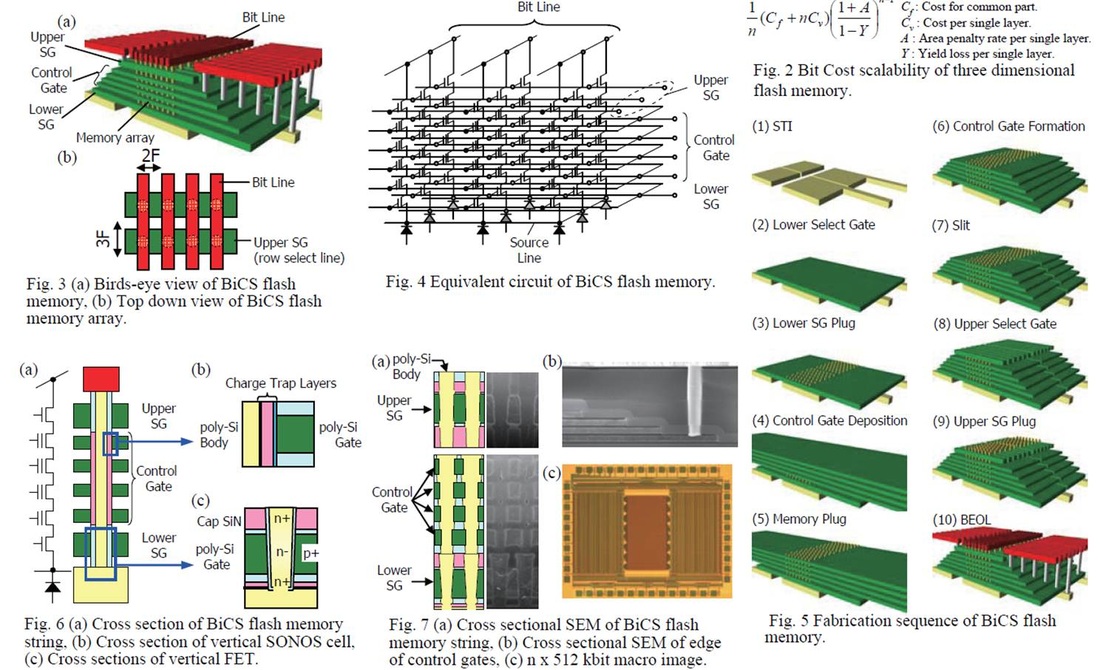
Figure 6: 3D NAND process steps, as described by Toshiba
The following are the key advantages of the 3D NAND:
- Fill the deep memory holes or trench slits. The top foreseeable challenges are ultra-high-aspect ratio (>40:1) conductor etch and dielectric etch with high etch selectivity to the hard mask
- With 3D NAND, scaling is no longer driven by lithography. The gate length is defined by deposition
- The key steps to 3D NAND are
- Fill the deep memory holes or trench slits. The top foreseeable challenges are ultra-high-aspect ratio (>40:1) conductor etch and dielectric etch with high etch selectivity to the hard mask
- 3D NAND is relatively straightforward for a DRAM maker since it has stacked SiO2 and polysilicon layers like a stacked capacitor DRAM, and trenches like a trench cell DRAM.
- 3D NAND is evolutionary, not revolutionary.
- The good news is continued cost reduction, smaller die sizes and more capacity.
- Installed NAND toolsets in the wafer Fabs can, for the most part, be reused, thereby extending the useful life of Fab equipment.
- 3D NAND technology is still basically NAND with all its inherent limitations of data reliability and performance: hence, generally well understood (evolutionary).
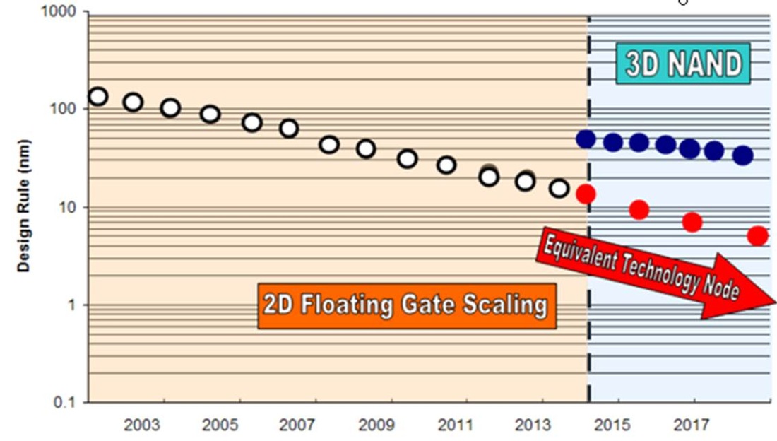
Figure 7: 3D NAND effect on design rules
Figure 7 describes the essence of the advantage of moving from 2D to 3D NAND. The adoption of 3D NAND technology will remove the burden from the Litho (and hence EUV) into the much easier process steps (deposition). Of course there are other advantages as described above.
It is not too difficult to see the similarity between the up and coming 3D NAND and the Monolithic 3D approach. As we describe in our web site (www.monolithic3d.com) the advanced technology patented by MonolithIC 3D Inc. enables the fabrication of Monolithic 3D Integrated Circuits with multiple stacked transistor layers and ultra-dense vertical connectivity. Thus, it appears monolithic 3D-ICs with 2 device layers provide benefits similar to a generation of conventional scaling. Furthermore, just as conventional scaling reduces feature sizes every generation, monolithic 3D opens the road for many years of continuous scaling by ‘folding’ once, twice, and so forth without necessarily reducing feature sizes.
It is not too difficult to see the similarity between the up and coming 3D NAND and the Monolithic 3D approach. As we describe in our web site (www.monolithic3d.com) the advanced technology patented by MonolithIC 3D Inc. enables the fabrication of Monolithic 3D Integrated Circuits with multiple stacked transistor layers and ultra-dense vertical connectivity. Thus, it appears monolithic 3D-ICs with 2 device layers provide benefits similar to a generation of conventional scaling. Furthermore, just as conventional scaling reduces feature sizes every generation, monolithic 3D opens the road for many years of continuous scaling by ‘folding’ once, twice, and so forth without necessarily reducing feature sizes.
- F. Masuoka et. al IEDM 1984 pp464-467
- F. Masuoka et. al IEDM 1987 pp552-555
- H. Tanaka et al., Symp. on VLSI Tech. Dig., pp 14-15, 2007


 RSS Feed