We have a guest contribution today from Israel Beinglass, the CTO of MonolithIC 3D Inc. Israel was at Applied Materials for almost two decades, and served as Chief Technology Officer and Chief Marketing Officer for many groups there.
.
- Completion of wafer size change from 200mm to 300mm
- We lived through 4 technology nodes: 90nm, 65nm, 45nm, and 32nm
- Channel stress both using selective epitaxial deposition and stressor films deposition became the standard mobility enhancement knob.
- High k Metal gate was introduced and though is not a the standard everywhere it is on the way to become a standard in the coming years


At this time the industry is utilizing double patterning as a fall back position due to the lack of a viable solution for EUV, which in turn forced manufacturers to buy more steppers and etchers.
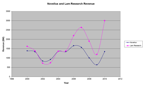
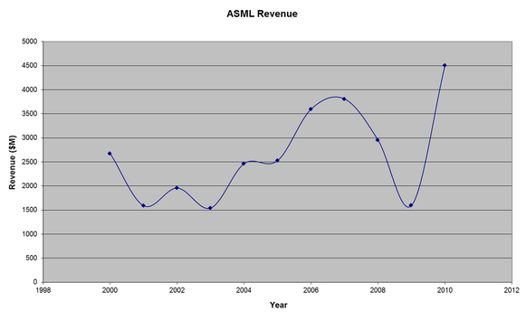
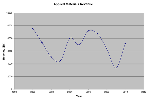
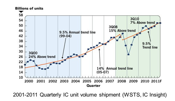
Let’s review again the reason why within a range of 10 years revenue of some leading companies didn’t grow at all, though the total number of units has gone up as well as the total semiconductor revenue. This is in spite of Applied Materials leading in PVD, Low k deposition, RTP, Epi and CMP. At the same time Novellus has a leading position in several CVD depositions and ECP.
The reasons for these are:
- Less Fabs are built in the world due to the success of the foundry business and consolidation in the memory business.
- Reuse of same equipment in new Fabs, as the equipment is being transferred instead of retired.
- Conversion of 200mm to 300mm, increasing by 2.5x the number of chips on each wafer, hence less equipment is needed.
- The throughput of most of the new equipment has gone up dramatically within the last decade by the equipment companies due to pressure from their customers.
In summary, in new Fabs, the Litho portion of the total expenses is getting larger and larger and the companies who are selling to this market will increase their % of the whole new Fab expenses.
In my next blog I will continue to develop these ideas and I will discuss several options of how the industry will continue on the Moore path: using double patterning, direct write, EUV, and 3D devices. Also we will revisit the effect these new technologies will have on the future revenue of equipment companies.


 RSS Feed