
We have a guest contribution today from Israel Beinglass, the CTO of MonolithIC 3D Inc. Israel discusses the foundry industry's history as well as its current landscape...
Today, we are all living in “the foundry world”. Almost all advanced node logic chips are made in foundries (excluding Intel and IBM). Let’s ask ourselves some tough questions regarding these.
1. The emergence of Fabless companies (e.g. Qualcomm, Broadcom, Altera, Xilinx)
2. The conversion of IDM companies from IDM to Fab-lite as an intermediate step to fully Fabless companies (e.g. AMD, LSI logic, Motorola, TI-non analog)
Let’s first review the history of foundries.
Foundry History-Phase one:
Originally the IC industry was practically all IDM (remember in the 80’s through the early 90’s Intel, National, Motorola, AMD, TI, IBM) that designed and manufactured their products. At that time there was a lot of “black magic” and each company developed their unique process and kept it close to their vest, while tweaking the process to optimize the final IC product. However as the time passed and engineers moved between different companies, they brought with them each others' process steps resulted in more standard and unified processes. Also, at the same time, design rules and scaling methodologies became the way of doing business, this allowed to separate design from manufacturing. Of course the introduction of EDA capabilities was instrumental to that development.
Morris Chang, a Texas Instruments executive, was recruited by the Taiwan government to help strengthen its semiconductor industry and became president of Taiwan’s Industrial Technology Research Institute in 1985. He founded the Taiwan Semiconductor Manufacturing Company (TSMC) in 1987 as the world’s first dedicated IC foundry company. By focusing on manufacturing other companies’ ICs, TSMC met the needs of chip manufacturers requiring outside contractors for overflow and specialty work and provided services for companies lacking the resources to do their own fabrication work. While there was skepticism concerning the viability of such a business model, Dr. Chang was persistent and was able to demonstrate its advantages. TSMC became the template for fabrication houses that followed such as UMC, Chartered, SMIC and Globalfoundries, and through Dr. Chang’s leadership TSMC developed into the largest silicon foundry in the world.
The creation of TSMC sparked the development of fabless IC companies during the 1990s. Dedicated foundries reduced the cost of entry for these companies by manufacturing their chips but without competing with them.
Foundry History-Phase two:
As the foundry business grew and became a winning model, a second phase started in the late ‘90s and early ’00s. The second phase started as the scaling became more aggressive (Moore’s law) and building new Fabs as well as the R&D costs skyrocketed. Most companies couldn’t afford these kinds of expenses. As the results of these many companies closed down their production facilities and moved their manufacturing to foundries. Some examples are LSI Logic, IDT, Motorola (Spun out Freescale), Atmel, AMD (Spun out GlobalFondries). Some of these activities were done in 2 steps. First, the concept of Fab-lite was introduced whereby a company sheds some of the production Fabs and moves to foundry and later on either leave it like that or totally close down manufacturing.
Current Foundry status
Figure 1 shows the overall foundry revenue and the annual growth rate from 2001 through 2011, and estimates for 2012 and 2013 (iSuppli).
- How did it happen and what can we learn from that?
- Is there any danger to the world semiconductor production?
- Do foundries have too much power over their customers?
- Why does one foundry control over 50% of the advanced logic device manufacturing?
1. The emergence of Fabless companies (e.g. Qualcomm, Broadcom, Altera, Xilinx)
2. The conversion of IDM companies from IDM to Fab-lite as an intermediate step to fully Fabless companies (e.g. AMD, LSI logic, Motorola, TI-non analog)
Let’s first review the history of foundries.
Foundry History-Phase one:
Originally the IC industry was practically all IDM (remember in the 80’s through the early 90’s Intel, National, Motorola, AMD, TI, IBM) that designed and manufactured their products. At that time there was a lot of “black magic” and each company developed their unique process and kept it close to their vest, while tweaking the process to optimize the final IC product. However as the time passed and engineers moved between different companies, they brought with them each others' process steps resulted in more standard and unified processes. Also, at the same time, design rules and scaling methodologies became the way of doing business, this allowed to separate design from manufacturing. Of course the introduction of EDA capabilities was instrumental to that development.
Morris Chang, a Texas Instruments executive, was recruited by the Taiwan government to help strengthen its semiconductor industry and became president of Taiwan’s Industrial Technology Research Institute in 1985. He founded the Taiwan Semiconductor Manufacturing Company (TSMC) in 1987 as the world’s first dedicated IC foundry company. By focusing on manufacturing other companies’ ICs, TSMC met the needs of chip manufacturers requiring outside contractors for overflow and specialty work and provided services for companies lacking the resources to do their own fabrication work. While there was skepticism concerning the viability of such a business model, Dr. Chang was persistent and was able to demonstrate its advantages. TSMC became the template for fabrication houses that followed such as UMC, Chartered, SMIC and Globalfoundries, and through Dr. Chang’s leadership TSMC developed into the largest silicon foundry in the world.
The creation of TSMC sparked the development of fabless IC companies during the 1990s. Dedicated foundries reduced the cost of entry for these companies by manufacturing their chips but without competing with them.
Foundry History-Phase two:
As the foundry business grew and became a winning model, a second phase started in the late ‘90s and early ’00s. The second phase started as the scaling became more aggressive (Moore’s law) and building new Fabs as well as the R&D costs skyrocketed. Most companies couldn’t afford these kinds of expenses. As the results of these many companies closed down their production facilities and moved their manufacturing to foundries. Some examples are LSI Logic, IDT, Motorola (Spun out Freescale), Atmel, AMD (Spun out GlobalFondries). Some of these activities were done in 2 steps. First, the concept of Fab-lite was introduced whereby a company sheds some of the production Fabs and moves to foundry and later on either leave it like that or totally close down manufacturing.
Current Foundry status
Figure 1 shows the overall foundry revenue and the annual growth rate from 2001 through 2011, and estimates for 2012 and 2013 (iSuppli).
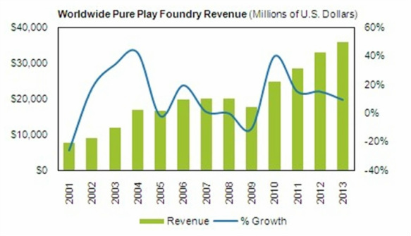
Figure 1: Worldwide Foundry Revenue (Source: iSuppli)
Figure 2 is a table showing 2010 revenue of the top 10 foundries in the world. It is very clear that TSMC is by far the 400lb gorilla in this game with close to 50% market share. The major players are TSMC, UMC, GlobalFoundries and SMIC. The second tier numbers 5-10 are mixed of specialty foundries like TowerJazz, Dongbu and MagnaChip as well as IBM which doesn’t make real efforts to gain market share and Samsung as a newcomer. If we exclude number 5-10 then TSMC has a startling 60% market share!!!!
Advanced technology nodes like 45nm, 32(22)nm and 22(20)nm require massive investment in new facilities, new equipment like steppers and other production tools. During the last few years the foundries did invest vast amount of money in this kind of equipment, this investment will have to continue assuming that they will try to extend the momentum of scaling down to 14nm and beyond.
Advanced technology nodes like 45nm, 32(22)nm and 22(20)nm require massive investment in new facilities, new equipment like steppers and other production tools. During the last few years the foundries did invest vast amount of money in this kind of equipment, this investment will have to continue assuming that they will try to extend the momentum of scaling down to 14nm and beyond.
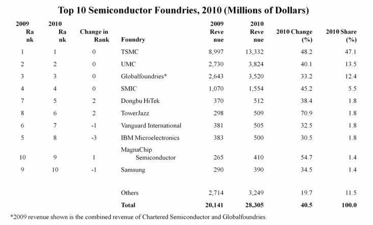
Figure 2: Top ten foundries (Source: Gartner).
At this point in time, it looks like TSMC is the overwhelming winner in the foundry business with a whopping 50% market share, an unprecedented situation (comparable maybe only to Intel’s position in the microprocessor arena). Looks like TSMC did everything right from the point of view of technology, customer service, production capabilities etc. At the same time the competitors are behind and it is not easy for them to close the gap.
Some of the questions that come to mind are the following:
Foundries and advanced packaging;
It has been recently reported that some of the foundries especially TSMC started to work on 2.5D silicon interposers. Looks like the 3D device concept is finally catching up after very long gestation time. 3D TSV is still a long shot since it is still complicated and lacks standardization.
Some of the questions that come to mind are the following:
- What about TSMC's customers? Aren’t they worried in case something happens like a massive earthquake, floods or other natural disasters, yield crashes or even political unrest?
- Another question is the capability of TSMC to raise prices. In some of the advanced nodes they have a big lead over their competitors hence they can charge premium prices.
Foundries and advanced packaging;
It has been recently reported that some of the foundries especially TSMC started to work on 2.5D silicon interposers. Looks like the 3D device concept is finally catching up after very long gestation time. 3D TSV is still a long shot since it is still complicated and lacks standardization.
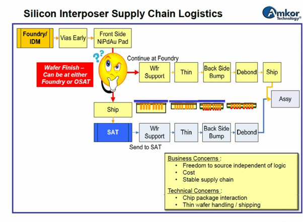
Figure 3: Logistics of Silicon Interposer Technology.
However the one step before real TSV, the so called 2.5D interposer, is getting some traction. As per this URL the cost at TSMC for a 2.5D is $10K at present!!! Obviously a high price. (http://semimd.com/blog/2011/11/18/foundries-extend-reach-into-packaging-fronts/). Figure 3 shows (as per Amkor) the steps and the supply chain logistics involved with the manufacturing of 2.5D silicon interposers - very complicated.
Looks like the solution that MonolithIC 3D Inc. suggests can level the paying field by un-leveling the IC from 2D to 3D. Reports suggest that every folding is equivalent to one generation of dimensional scaling. Many of the foundries that do not have the volume to justify the enormous investment required for the next generation fab, could instead enhance their existing lines with monolithic 3D technology. By offering 3D options to their customers, they could build devices competitive with the leading edge foundries and leverage well depreciated manufacturing lines. Please tune in to a future blog where I will address some of these issues.
Looks like the solution that MonolithIC 3D Inc. suggests can level the paying field by un-leveling the IC from 2D to 3D. Reports suggest that every folding is equivalent to one generation of dimensional scaling. Many of the foundries that do not have the volume to justify the enormous investment required for the next generation fab, could instead enhance their existing lines with monolithic 3D technology. By offering 3D options to their customers, they could build devices competitive with the leading edge foundries and leverage well depreciated manufacturing lines. Please tune in to a future blog where I will address some of these issues.


 RSS Feed