
We have a guest contribution today from Israel Beinglass, the CTO of MonolithIC 3D Inc. Israel was at Applied Materials for almost two decades, and served as Chief Technology Officer and Chief Marketing Officer for many groups there.
In late September I published the first installment of my set of 2 parts regarding the status of semiconductor equipment manufacturing. I’d like to continue my analysis and discuss where there will be growth in the industry for the next few years, how, and why. Let’s first review where there will no growth or actually shrinking.
FRONT END
-Gate and Gate electrode formation: Obviously this is a new application waiting to be implemented across the board on all advanced logic devices. At the time this blog is written, only Intel has mastered this application while the rest of the world is trying to catch up. However, I think eventually they will get it and the process will become ubiquitous. The problem, of course, is that this is a single pass in the process flow (unlike interconnect), so, yes this is a new application and ALD tools will be sold by ASMI who is the leader in this field (many already have been sold) but in the grand scheme of things, this will not have a big effect on the total equipment business.
-Implant: This is probably the only section of the equipment industry that will suffer a substantial reduction within the next few years. The reason for that is that all the new advanced devices use less and less implant due to simple device formation. Also several S/D will be formed using doped epi growth that will cut major implant steps. In that case it is not clear what is the benefit for Applied Materials purchasing Varian for top $$ as a future growth industry. There might be some increase in PLAD (Plasma doping) tools usage for certain new applications (beyond poly doping for DRAM). Some applications will be in the FINFET doping or generic material modification processes- a process long been in the making.
-Thermal processing: RTP and millisecond anneal will continue to be used. As the time will go by and more advanced devices will be built using smaller and smaller geometry, the RTP portion of the thermal processing will shrink while the portion of the millisecond anneal will grow. Looks like Ultratech with the Laser Annealing will benefit from this kind of a trend.
BACK END
-Metal layers: Looks like there will not be a major change in the way the industry is putting down metal (copper, dual damascene etc). The number of interconnect layers has not grown anymore like it used to grow several years ago.
-Dielectric: The name of the game is to reduce the dielectric constant of the dielectric layers (Low k) beyond the value currently used (2.5), though it is a very difficult task because of reliability issues arising from the softness of the super low k materials.
-Even if a new generation of low k materials emerges, it will not make a dent in the demand for back end low k material deposition, since most of the tools already exist and probably will just need to change precursor.
CMP: Some increase could result from more CMP processing in the front end relating to the high k /metal gate process sequence.
FUTURE GROWTH
Well, in that case where is the growth going to be…? It will be in the Patterning processes.
The main reason for that is the lack of EUV availability to bring a mature tool to production at the 22(20) nm technology node. Looks like “double patterning” and all the associate technology around it is a reasonable working solution. This approach is here to stay at least for another one or two generations.
When in the past people refer to patterning they meant only the resist/expose/etch steps. The introduction of double patterning and in the future quadruple pattering brings new steps of deposition (spacer) and for masking, ARC (Anti Reflecting Coating) and hard mask. So the future growth for the equipment industry will all relate to “patterning”.
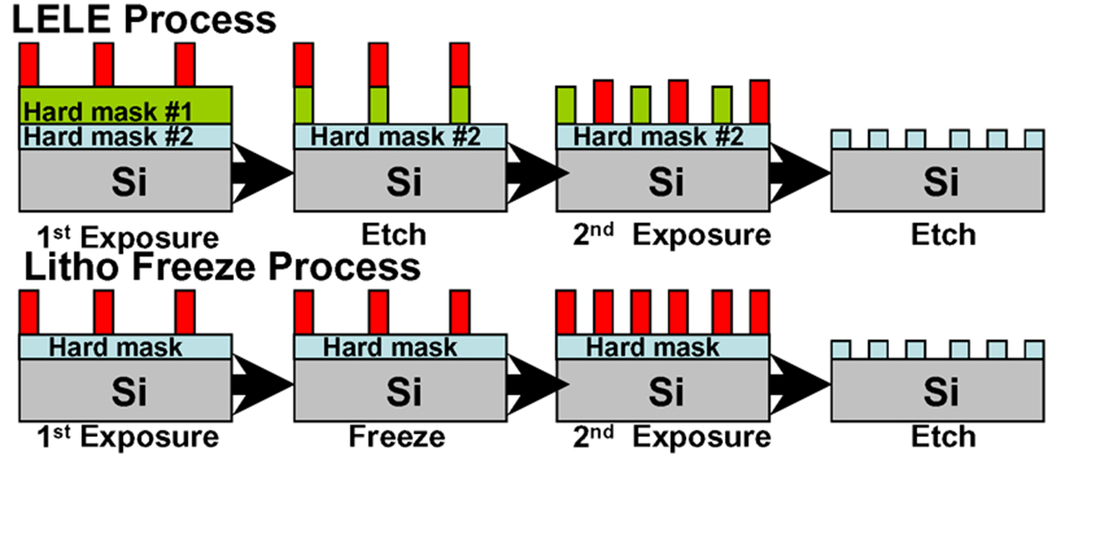
Figure 1 Using masking only approach
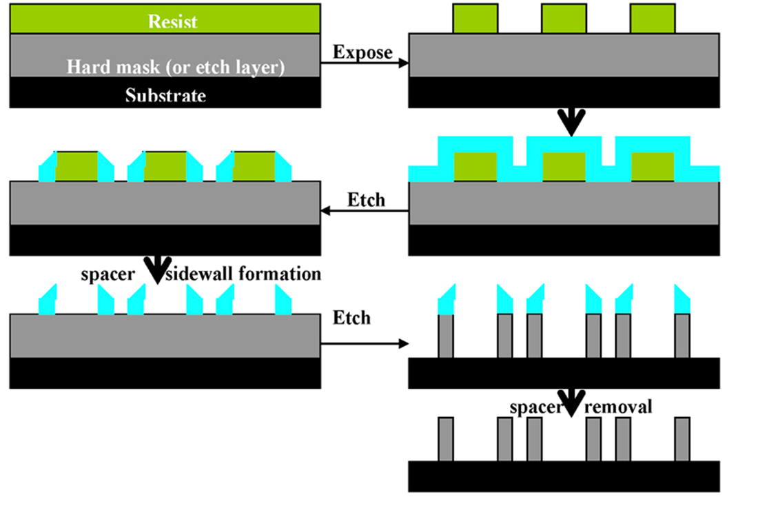
Figure 2 Using spacer
There are many approaches that the industry is looking at, some of them are depicted in figures 1 and 2. Figure 1 is using masking only approach while figure 2 is using spacer.
The equipment companies that will benefit from this trend in the patterning will be ASML that will be able to sell more steppers. In the etch arena Lam and TEL will be able to sell more etch tools and in the deposition area Applied Materials and Novellus will participate in the Hard mask, ARC and sidewall spacer deposition. However, many companies already own these kinds of tools so they will have to upgrade it somewhat or will have to add several new tools.
Of course KLA-Tencor will benefit from this development since many more of their capabilities will be needed hence more metrology and inspection tools will be sold.
Double patterning (or quadruple) is not coming for free, all these extra steps will increase the price of a fully processed wafer, which will put extra burden on the chip manufacturing since raising prices is not what the consumers would like to deal with at any time.


 RSS Feed