We would also like to share with you our latest participation at the S3S 2015 Conference by providing you with a video tutorial: S3S Video/presentation on Game Changing 2.0
|
Happy Thanksgiving from MonolithIC 3D Inc. Team.
We would also like to share with you our latest participation at the S3S 2015 Conference by providing you with a video tutorial: S3S Video/presentation on Game Changing 2.0
0 Comments
The Path to Alternative Scaling is Now Open
IEEE S3S 2015 could be the turning point for monolithic 3D. During Oct. 4-7 we will have the option to get a short course, invited and selected presentations from a broad range of the industry representatives. They include major vendors such as Qualcomm, Global Foundries and Applied Materials; leading research organization like CEA Leti, Taiwan National Applied Research Labs, German IMS Chips, NASA; leading Universities like Berkeley and Stanford; start-ups like SiGen and MonolithIC 3D.
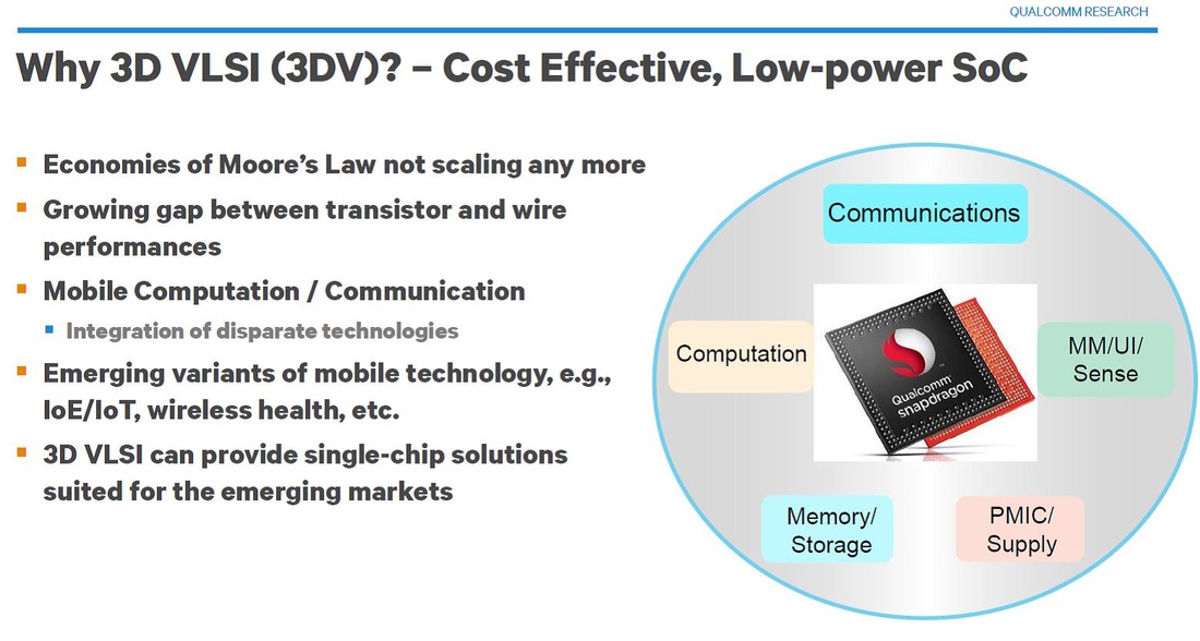
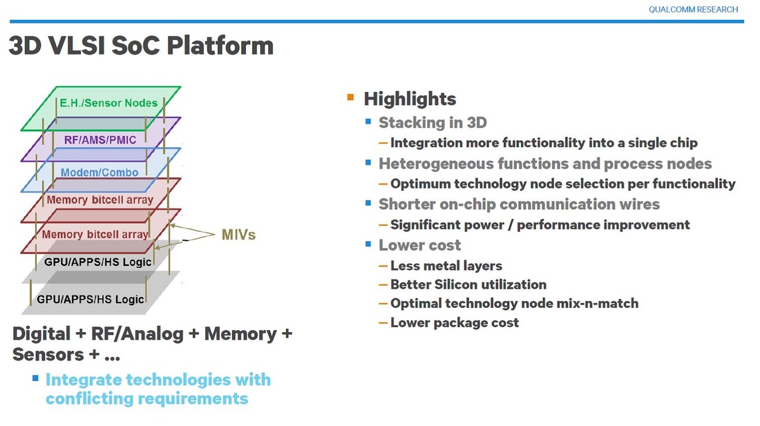
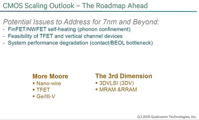
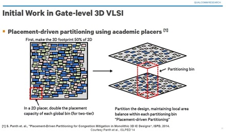
In its tutorial session Qualcomm will explain why it is investing and promoting 3D VLSI (3DV) as an alternative scaling technology, as is illustrated by the following two slides:
Yet many people still have doubts as is reflected by the title of the panel we were invited to participate in -- “Monolithic 3D: Will it Happen and if so…” -- at the IEEE 3D-Test Workshop Oct. 9, 2015.
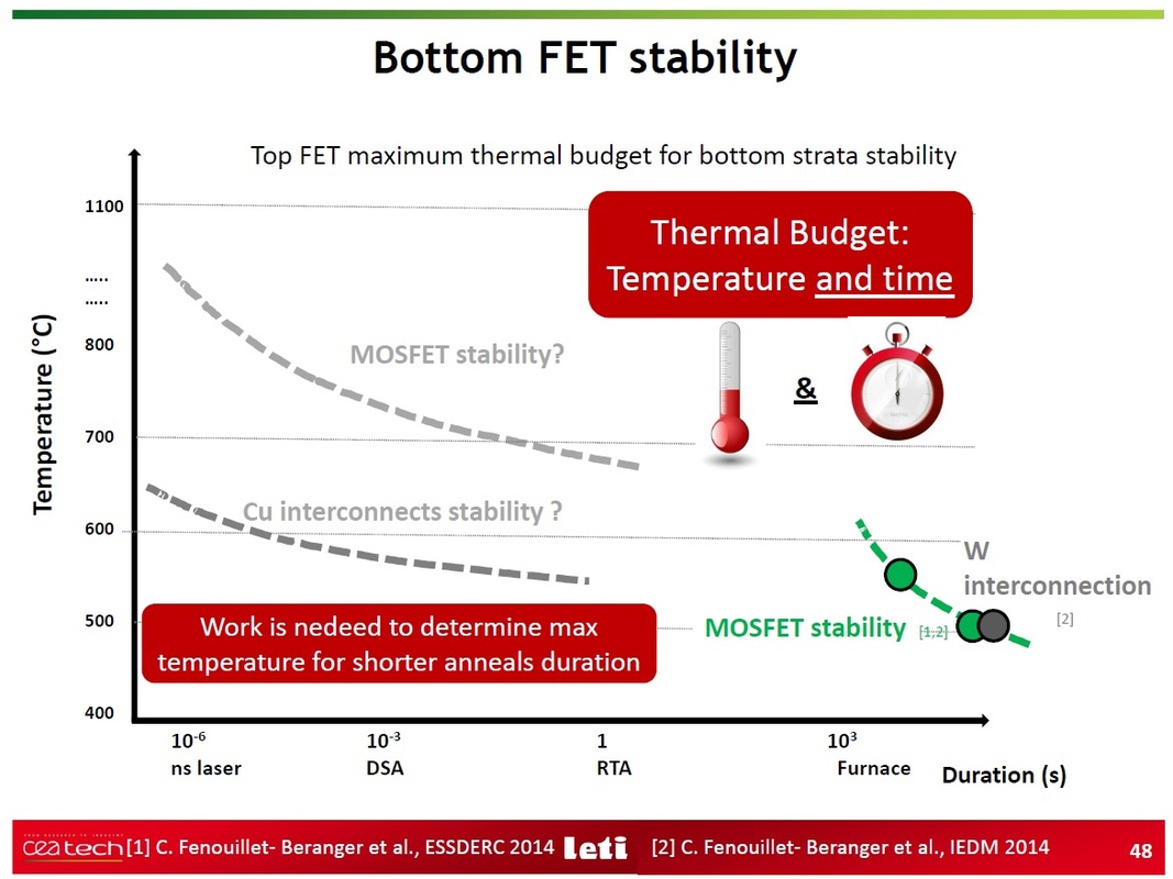
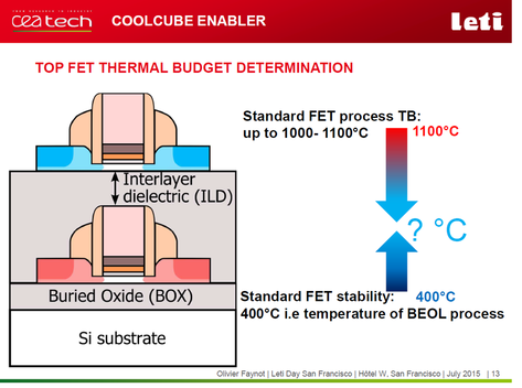
The doubts likely relate to the technology challenge that is illustrated in the following slide:
The question, in short, is how we can add more transistors monolithically interconnected to the underlying transistors without exceeding the thermal budget for the underlying transistors and interconnect.
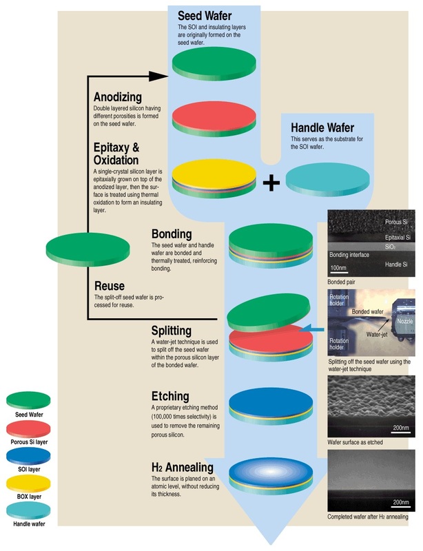
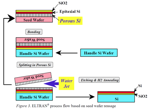
The current paths to monolithic 3D involve major changes to the front line process flow and require the development of a new logic transistors. The big concern is that leading edge vendors are too busy with dimensional scaling and if anything else could be done it seems that FD-SOI would be it, while trailing edge fabs are, in most cases, avoiding any major transistor process development. The recent failure of Suvolta could be an indication of this reality. Hence the importance of Game-Changing 2.0, a major technology innovation to be unveiled on Wednesday by MonolithIC 3D in a paper titled: “Modified ELTRAN® - A Game Changer for Monolithic 3D”. The paper will present a novel use of the ELTRAN® process developed by Canon about 20 years ago primarily for SOI applications. Using ELTRAN (Epi. Layer Transfer) techniques, a substrate could be prepared enabling any fab to simply integrate a monolithic 3D device without the need to change its current front-line fab process. This flow is further simplified and could be integrated with the monolithic 3D flow introduced last year that leverages the emerging precision bonders, such as EVG’s GeminiÒ XT FB. This flow provides a natural path for product innovation and an unparalleled competitive edge to its adopters. In addition, this game-changing breakthrough offers a very cost-competitive flow. The following chart illustrates the original use of ELTRAN process for the fabrication of SOI wafers:
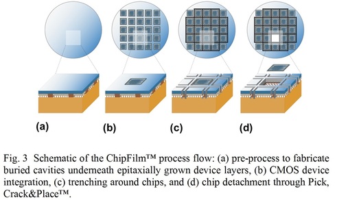
In the “Invited Talks on M3DI” at the conference we will have an opportunity to learn from the inventor of the ELTRAN process, Dr. Takao Yonehara, currently with Applied Materials, in his “Epitaxial Layer Transfer Technology and Application” talk. Prior to Applied Materials Dr. Yonehara worked with Solexel, a Silicon Valley startup, to deploy the ELTRAN process for low cost solar cell fabrication. Yonehara’s talk will be followed by Prof. Joachin Burghartz of Institute for Microelectronics in Stuttgart, discussing “Ultra-thin Chips for Flexible Electronics and 3D ICs” that uses a variation of such flow in small scale production.
The semiconductor industry is bifurcating these days into a segment that follows aggressive scaling for few super-value applications supported by very few vendors, while the bulk of the industry is enhancing old fabs targeting mainstream applications and the emerging IoT opportunities. Further enhancing these older fabs with monolithic 3D offers a most effective return on investment. Game-Changing 2.0 means that without a need for major process R&D efforts or new equipment, the path for 3D scaling is now open with enormous advantages for IoT. Accordingly, my answer to the original question above is summarized by the title of our invited talk at the IEEE 3D-Test Workshop:“Monolithic 3D is Already Here – the 3D NAND – and Now it would be Easy to Adapt it for Logic.” In addition the other division – SOI and SubVt provide good complementing technology updates for the power-performance objectives that are so important for these emerging markets. Do come to the S3S and enjoy unique key technologies update with the great wine and country pleasures of Sonoma Valley.
Game-Changing 2.0 @ IEEE S3S
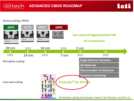
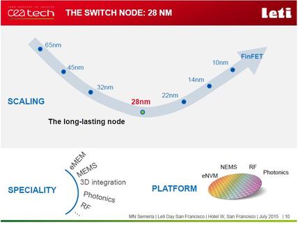
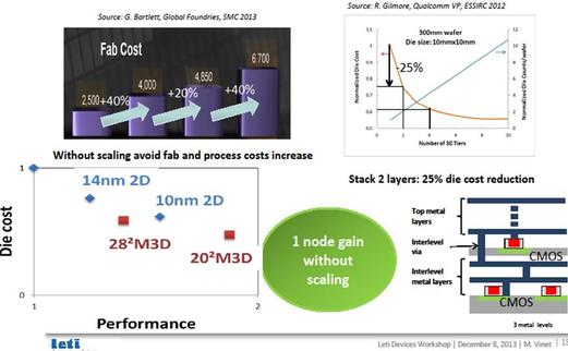
We were invited to join a panel session titled: "Monolithic 3D: Will it Happen and if so..." at IEEE 3D-Test Workshop Oct. 9th, 2015. So we are happy to see monolithic 3D on the title, but then the title also suggests that the industry is wondering is it real or is it a pipe dream. The doubts are in opposition to companies such as Qualcomm who strongly advocate it, and the support CAE which Leti, in collaboration with ST Micron and IBM,are presenting monolithic 3D as the "low-cost scaling" for 2018. See chart below from July 2015 Leti Day.
The doubts might relate to the technology challenge illustrated by the following slide:
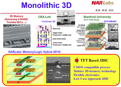
The upcoming IEEE S3S Conference 2015 in Sonoma, CA, on October 5th thru 8th provides comprehensive coverage of R&D activities in the monolithic 3D space. It starts with short courses on Monday. On Tuesday there will be a planery talk - "Sustaining the Silicon Revolution: From 3-D Transistors to 3-D Integration" by Prof. Tsu-Jae King Liu, followed by "3D-Invited Monolithic 3D Alternative Technologies" session with representatives of Qualcomm, CEA Leti, Taiwan National Nano Device Laboratories, Stanford University and UCLA presenting and updating on the state of monolithic 3D technologies currently being developed arround the world as being illustrated in the following slide:
Then on Wednesday we would have an additional session of “Invited Talks on M3DI” followed by a “Selected Papers on M3DI” session.
In short the most comprehensive technical event on the emerging monolithic 3D technologies. Yet – the question “Monolithic 3D: Will it Happen…” is still being asked. The concerns are that the leading edge vendors are too busy these days still with dimensional scaling and if anything else could be done it seems that FD-SOI would be it; while trailing edge fabs, are in most cases, avoiding any major transistor process development. The recent failure of Suvolta could be an indication of this reality. Here comes Game-Changing 2.0. A major technology innovation to be unveiled on Wednesday by MonolithIC 3D in a paper titled: “Modified ELTRAN® - A Game Changer for Monolithic 3D”. This paper will present a novel use of the ELTRAN® process developed by Canon Inc. about 20 years ago primarily for SOI applications. Using ELTRAN (Epi. Layer Transfer) techniques, a substrate could be prepared enabling any fab to simply integrate a monolithic 3D device without the need to change the current frontline fab process. This flow is further simplified and could be integrated with the game changing monolithic 3D flow introduced last year which leverages the emerging precision bonders, such as EVG’s Gemini® XT FB. This flow provides a natural path for product innovation and an unparalleled competitive edge. In addition, this game-changer breakthrough offers a very cost competitive flow. The following chart illustrates the original use of ELTRAN process for the fabrication of SOI wafers:
In the “Invited Talks on M3DI” we will have an opportunity to learn from the inventor of the ELTRAN process Dr. Takao Yonehara, currently with Applied Materials, in his talk “Epitaxial Layer Transfer Technology and Application”. Prior to Applied Materials Dr. Yonehara worked with Solexel, a Silicon Valley start up, to deploy the ELTRAN process for low cost solar cell fabrication. This talk would be followed by Prof. Joachin Burghartz of Institute for Microelectronics Stuttgart, talk on “Ultra‐thin Chips for Flexible Electronics and 3D ICs” where they use a variation of the flow in small scale production.
The semiconductor industry are bifurcating these days into one a segment that follows aggressive scaling for few super-value applications supported by very few vendors, while the bulk of the industry is enhancing old fabs while targeting the main stream applications and the emerging IoT opportunities. Further enhancing these older fabs with monolithic 3D would be a most effective return on investment. As indicate by the CEA slide above – “low cost scaling” and by a paper to be presented by Global Foundries showing monolithic 3D provides Power-Performance-Area (PPA) equivalent to dimension scaling at fraction of the cost. The Game-Changing 2.0, mean that without need for major process R&D efforts or new equipment the path for 3D scaling is now open with enormous advantages for IoT. And accordingly my answer to the above question is encompassed in the title of the invited talk prior to the panel “Monolithic 3D is Already Here – the 3D NAND – and Now it would be Easy to Adapt it for Logic” In addition the other division – SOI and SubVt provide good complementing technology updates for the power performance objectives that are so important for these emerging markets. So do come to the S3S and enjoy unique key technologies update with the great wine and country pleasures of Sonoma Valley.
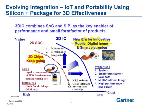
The forthcoming IEEE S3S Conference 2015 ,Sonoma, CA, on October 5th thru 8th, will focus on key technologies for the IoT era. It is now accepted that the needs for the emerging IoT market are different from those which drive the high volume PC and Smart-Phone market. The following Gartner slide illustrates this industry bifurcation where traditional mass products follow the – ever more expensive – scaling curve, while IoT devices, with their focus on cost, power, flexibility and accessibility, will seek place near its minimum.
The current high volume is focus on handful of foundries and SoC vendors driving a handful of designs at extremely high development cost each, processed at the most advanced nodes, with minimal processing options. In contrast, the emerging IoT market is looking for older nodes with lower development costs, broad range of process options, with many more players both at the foundry side and the design side.
For the IoT market the key enabling technologies are extreme low power, as enabled by SOI and sub-threshold design, integrating with multiple sensor technologies and communication technologies that ca be enabled by 3D integrations. All of these combined in forming the IEEE S3S unified conference. This year conference includes many exciting papers and invited talks. It starts with three plenary talks:
Quoting Jim Walker, Research VP at Gartner presented on the “Foundry vs. SATS: The Battle for 3D Wafer Level Supremacy”. He argued 3D ICs are the key enabler of performance and small form factor of products required for IoT.
Hence the coming IEEE S3S conference provides important opportunity to catch up and learn about these technologies. Let me share with you some nuggets from the monolithic 3D integration part of the conference: Prof. Joachin Burghartz of the Institute for Microelectronics Stuttgart will deliver an invited talk on “Ultra‐thin Chips for Flexible Electronics and 3D ICs” that will present a process technology to fabricate flexible devices 6-20 micron thin. This process flow is currently in manufacturing in their Stuttgart fab, as described below;
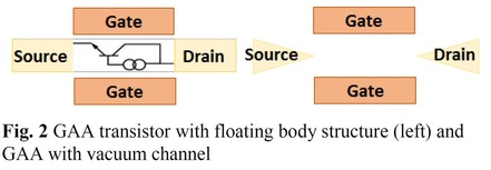
Another interesting discussion will be presented by NASA scientist Dr. Jin-Woo Han who will describe “Vacuum as New Element of Transistor”. These transistors are made of “nothing” and could be constructed within the metal stack, forming monolithic 3D integration with silicon-based fabric underneath.
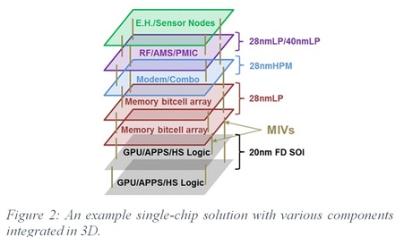
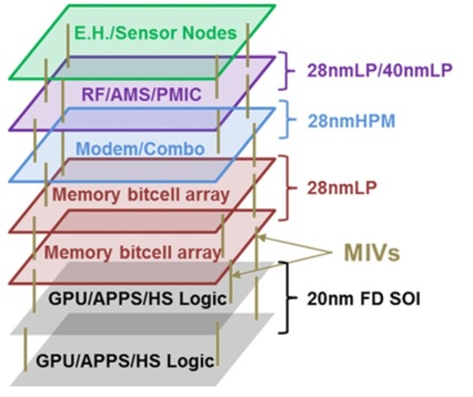
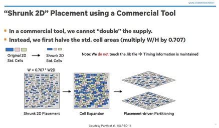
In his invited talk titled “Emerging 3DVLSI: Opportunities and Challenges” Dr. Yang Du will share with us Qualcomm views on monolithic 3D IC which they term 3DVLSI and could be illustrated by the following figure which seems very fitting for IoT applications
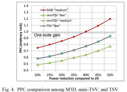
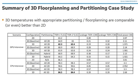
Globalfoundries will present joint work with Georgia Tec. titled “ Power, Performance, and Cost Comparisons of Monolithic 3D ICs and TSV-based 3D ICs”. This work again shows that monolithic 3D can provide a compelling alternative to dimension scaling as illustrated by the following chart.
We will present “Modified ELTRAN® - A Game Changer for Monolithic 3D” that shows a practical flow for exiting fab to process monolithic 3D devices using their exiting transistor process and equipment. This flow leverages the work done by Canon about 20 years back called ELTRAN, for Epitaxial Layer Transfer. The following slide illustrates the original ELTRAN flow.
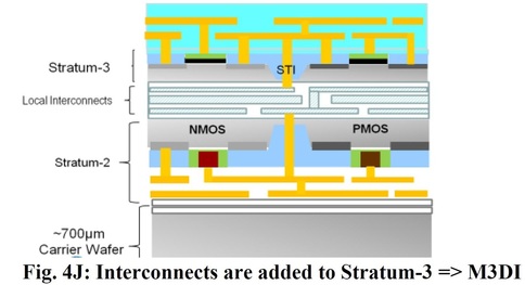
By deploying the elements of this proven process, a multilayer device could be built first by processing a multilayer transistors fabric at the front end of line, and then process the metal stacks from both top and bottom sides.
The conference includes many more interesting invited talks and papers covering the full spectrum of IoT enabling technologies. In addition, the conference offers short course on SOI application and monolithic 3D integration, and a fundamental class on low voltage logic. New technologies are an important part of the future of semiconductor industry, and a conference like the S3S would be a golden opportunity to step away for a moment from the silicon valley, and learn about non-silicon and silicon options that promise to shape the future.
The forthcoming IEEE S3S Conference 2015 ,Sonoma, CA, on October 5th thru 8th, will focus on key technologies for the IoT era. It is now accepted that the needs for the emerging IoT market are different from those which drive the high volume PC and Smart-Phone market. The following CEA Leti slide illustrates this industry bifurcation where traditional mass products follow the – ever more expensive – scaling curve, while IoT devices, with their focus on cost, power, flexibility and accessibility, will seek place near its minimum.
The current high volume is focus on handful of foundries and SoC vendors driving a handful of designs at extremely high development cost each, processed at the most advanced nodes, with minimal processing options. In contrast, the emerging IoT market is looking for older nodes with lower development costs, broad range of process options, with many more players both at the foundry side and the design side.
For the IoT market the key enabling technologies are extreme low power, as enabled by SOI and sub-threshold design, integrating with multiple sensor technologies and communication technologies that ca be enabled by 3D integrations. All of these combined in forming the IEEE S3S unified conference. This year conference includes many exciting papers and invited talks. It starts with three plenary talks:
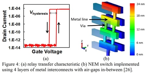
Prof. Tsu-Jae King will present in her talk an extremely low power nano-mechanical switch that could be fabricated within the metal stack. The slide below describes some of its characteristics.
Prof. Joachin Burghartz of the Institute for Microelectronics Stuttgart will deliver an invited talk on “Ultra‐thin Chips for Flexible Electronics and 3D ICs” that will present a process technology to fabricate flexible devices 6-20 micron thin. This process flow is currently in manufacturing in their Stuttgart fab, as described below;
Another interesting discussion will be presented by NASA scientist Dr. Jin-Woo Han who will describe “Vacuum as New Element of Transistor” As shown below
These transistors are made of “nothing” and could be constructed within the metal stack, forming monolithic 3D integration with silicon-based fabric underneath.
The conference includes many more interesting invited talks and papers covering the full spectrum of IoT enabling technologies. In addition, the conference offers short course on SOI application and monolithic 3D integration, and a fundamental class on low voltage logic. Among the papers we will present “Modified ELTRAN® - A Game Changer for Monolithic 3D” that shows a practical flow for exiting fab to process monolithic 3D devices using their exiting transistor process and equipment. This flow leverages the work done by Canon about 20 years back called ELTRAN, for Epitaxial Layer Transfer. By deploying the elements of this proven process, a multilayer device could be built first by processing a multilayer transistors fabric at the front end of line, and then process the metal stacks from both top and bottom sides. The following slide illustrates the resulting monolithic 3D structure.
New technologies are an important part of the future of semiconductor industry, and a conference like the S3S would be a golden opportunity to step away for a moment from the silicon valley, and learn about non-silicon and silicon options that promise to shape the future.
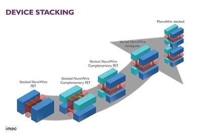
This year Semicon West had a clear undertone – the roadmap forward is 3D IC. Yes, we can and we will keep pushing dimensions down, which for a few applications would be attractive, but for most designs the path forward would be “More than Moore.” As Globalfoundries' CEO Jha recently voiced: “it's clear that More-than-Moore is now mainstream rather than niche. …Really it is leading-edge pure digital that is the niche. Instead the high-cost leading edge processes are really niche processes optimized for applications in data centers or for high computational loads, albeit niches with volumes of hundred of millions of units per year.” Similarly, EE Times editor Rick Merritt subtitled his Semicon West summary Roadmap being drawn for chip stacks. All this is nicely illustrated by the following slide presented by An Steegen of IMEC for their pre-Semicon Technology Forum:
Leti, the other major semiconductor R&D organization, has gone even further by dedicating its Semicon West day entirely to 3D technologies, as can be seen in the following invitation:
2015-LetiDay-SanFrancisco
GOING VERTICAL WITH LETI: Solutions to new applications using 3D technologies
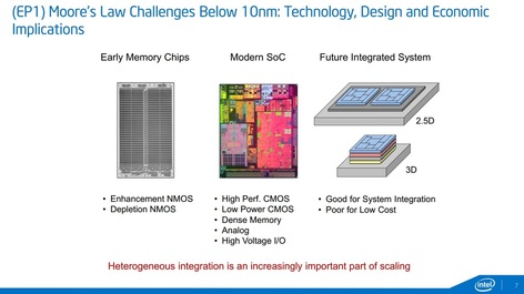
A similar view was also presented by Intel. Quoting Jeff Groff from his summary of Intel’s Q2 call: “In summary, it seems that Intel is executing fairly well on the process technology side of the business considering the ever increasing difficulty of pushing forward with Moore's Law. We can expect exciting new structures and materials (just maybe not at 10nm) and an increasing importance of 3-D structures in both logic and memory fabrication.” This echoes our blog Intel Calls for 3D IC, and was recently voiced by Intel’s process guru Mark Bohr: “Bohr predicted that Moore's Law will not come to an abrupt halt, but will morph and evolve and go in a different direction, such as scaling density by the 3D stacking of components rather than continuing to reduce transistor size.” It is also illustrated by his slide from ISSCC earlier this year.
The two concerns regarding 3D IC stacking using TSV are (a) Cost, noted in the slide above “Poor for Low Cost”, and (b) Vertical connectivity, as voiced by Mark Bohr: “Intel’s Bohr agrees that 3D structures will become more important. He said the kind of through-silicon vias used for today’s chip stacks need to improve in their density by orders of magnitude.”
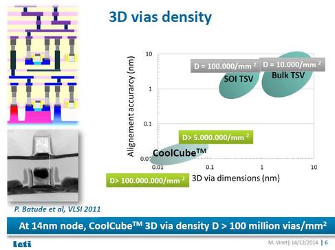
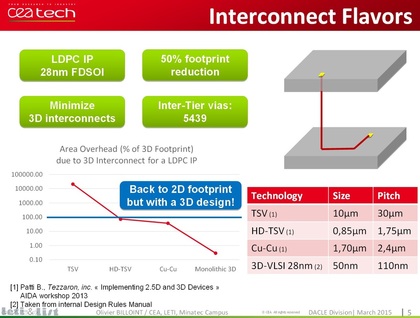
These limitations are the driver behind the efforts to develop monolithic 3D technology. Monolithic 3D would provide a very cost effective alternative to dimensional scaling with 10,000x higher than TSV vertical connectivity, as illustrated by the following two slides of CEA Leti.
Prof. Subhasish Mitra of Stanford assesses a 1,000x improvement in energy efficiency using monolithic 3D. His summary at a Semicon West keynote panel: “We have an opportunity for a thousand-fold increase in energy efficiency…from collaboration between dense computing and memory elements and dense 3-D integration of them.”
While stacking using TSV does not require any change to the transistor (‘front-line’) process flow, all monolithic 3D process flows until recently required a significantly new transistor formation flow. Since the transistor process is where the majority of the R&D budget and talent is being allocated, and carries with it fresh reliability concerns, the industry has been most hesitant with respect to monolithic 3D adoption. Yet in this recent industry gathering there is a sense that industry wide interest is building up for 3D technologies. The success of 3D NAND as the first monolithic 3D industry wide adoption could help this new interest build even faster. There is room for even more excitement. A recent technology breakthrough, first presented in IEEE S3S 2014 conference (Precision Bonders - A Game Changer for Monolithic 3D) introduced a game changer in the ease of monolithic 3D adoption. Enhancement of this breakthrough will be presented in this year’s IEEE S3S 2015. This new monolithic 3D flow allows the use of the existing fab transistor process for the fabrication of monolithic 3D devices, offering a most attractive path for the industry future scaling technology. P.S. A good conference to learn about these new scaling technologies is the IEEE S3S ‘15, in Sonoma, CA, on October 5th thru 8th, 2015. CEA Leti is scheduled to give an update on their CoolCube program, three leading researchers from Berkeley, Stanford and Taiwan’s NLA Lab will present their work on advanced monolithic 3D integration technologies, and many other authors will be talking about their work on monolithic 3DIC and its ecosystem. 
We have a guest contribution from Zvi Or-Bach, the President and CEO of MonolithIC 3D Inc.
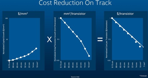
Vivek Singh, an Intel fellow, in his DAC 2015 keynote Moore's Law at 50: No End in Sight presented again the Intel chart below suggesting straight (log) line transistor cost reduction with dimensional scaling. In fact, his cost/transistor drop even seems to accelerate beyond the linear at 14 and 10 nanometers.
Vivek Singh, an Intel fellow, in his DAC 2015 keynote Moore's Law at 50: No End in Sight presented again the Intel chart below suggesting straight (log) line transistor cost reduction with dimensional scaling. In fact, his cost/transistor drop even seems to accelerate beyond the linear at 14 and 10 nanometers.
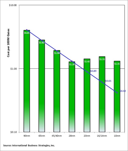
Less than a week later, Handel Jones (IBS) in his blog 10nm Chips Promise Lower Costs published an update down to 10nm of his well-known chart, presented below, of transistor cost with scaling.
Yes, 10 nm transistor cost is a bit less than that of the 16/14nm node, but still higher than that of the 28nm node and clearly showing that the historical cost reduction of 30% per node stopped at 28nm node. From that point on Handel Jones’ cost projections have been either flat or even a bit higher. Clearly, those charts are in a striking contradiction!
The IBS chart had been supported by the other foundries and their customers, as illustrated by quotes such as the following: “Samsung spent several years developing its 14nm technology and debating which process node it would invest in after 28nm. Low expects that 28nm will still be a popular process node for years to come because of its price…The cost per transistor has increased in 14nm FinFETs and will continue to do so, …”(http://www.eetimes.com/document.asp?doc_id=1326369), “Qualcomm is looking to monolithic 3D and smart circuit architectures to make up for the loss of traditional 2D process scaling as wafer costs for advanced nodes continue to increase. .. Now, although we are still scaling down it’s not cost-economic anymore” Karim Arabi, Qualcomm VP of engineering, DAC 2014 Keynote While the Intel chart Y axis has nominal values, we can plot Intel’s straight line cost reduction on the IBS chart as illustrated below on a half log scale:
Before jumping to our assessment of the cost difference between the green bars and Intel’s blue line, I’d like to direct you to a very detailed comment made by the “IJD” reader to Handle Jones’ blog. IJD suggests that Intel cost reduction could be explained by Intel’s very high starting point “since they effectively have a monopoly in one of the highest-margin highest volume chip markets which is x86 CPUs.”
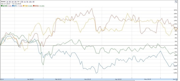
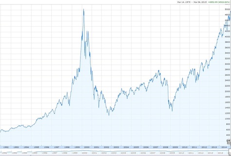
Intel has repeatedly used their chart in effort to promote their foundry business in competition with TSMC and in the process won the Altera business. Consequently, it seems important that we should compare Intel’s costs as illustrated by the blue line vs. the green bars as reported by the rest of the industry. We should consider the following points: 1. The Intel chart, while illustrating a simple formula, does seem logically faulty. The exponentially escalating cost of wafers needs to be neutralized by exponentially escalating scaling beyond the historical 0.7x scaling. Yet the major driver of wafer cost is lithography and it seems illogical to further reduce wafer cost by doing even more of it. Specifically, the escalating wafer cost below 28nm is driven by the need of double patterning and processing of few critical layers. Intel approach means that more layers would become critical and would need double patterning, driving the cost even higher. 2. A $0.42 per transistor vs. $1.31 per transistor should have won Intel far more foundry business, yet their major win was a very high margin vendor – Altera, and the rumor was that Altera was planning to go back to TSMC for the 10nm node. Foundry business is extremely competitive, as the customer owns the product IP and can choose the lowest cost foundry in order to win the extremely competitive end-market such as the smart phone market. 3. Intel’s $0.42 per transistor vs. the industry’s $1.31, combined with Intel’s command of the 86x CPU architecture, should have won Intel far more success in the Tablet market. 4. Looking at the last 6 months of Intel stock chart (below) in comparison to TSMC, Qualcomm and Nvidia does not show any market forecast for Intel future business resulting from its ability to beat its competitors by more than 3x the manufacturing cost. While Intel had consistently been the process technology leader, there is no special know-how or other unique advantage that could allow Intel to have 3x better costs than its competitors.
All we can do now is watch the market evolve and eventually tell us how the gap between these widely different cost estimates will be bridged.
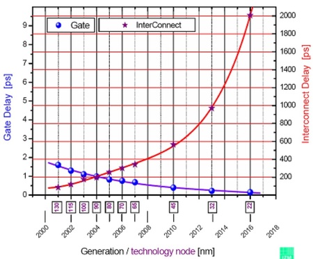
In any event, it is clear that Intel’s solution to the escalating cost of lithography is not sustainable. Over-scaling interconnect on its own, as Intel has sometimes hinted at, is extremely problematic because interconnect RC delays are increasing exponentially with scaling. This is nicely illustrated in the Applied Materials chart below.
Source: B. Wu, A. Kumar, Applied Materials
The only visible solution for the coming decade is monolithic 3D. Quoting Geoffrey Yeap, VP of Technology at Qualcomm, at his invited paper at IEDM 2013: “Monolithic 3D (M3D) is an emerging integration technology poised to reduce the gap significantly between transistors and interconnect delays to extend the semiconductor roadmap way beyond the 2D scaling trajectory predicted by Moore’s Law.” And even Intel’s process guru Mark Bohr seems to have come around: “Bohr predicted that Moore's Law will not come to an abrupt halt, but will morph and evolve and go in a different direction, such as scaling density by the 3D stacking of components rather than continuing to reduce transistor size.” (http://www.v3.co.uk/v3-uk/news/2403113/intel-predicts-moores-law-to-last-another-10-years)
P.S.
A good conference to learn about these new scaling technologies is the IEEE S3S ‘15, in Sonoma, CA, on October 5th thru 8th, 2015. CEA Leti is scheduled to give an update on their CoolCube program, three leading researchers from Berkeley, Stanford and Taiwan’s NLA Lab will present their work on advanced monolithic 3D integration technologies, and many other authors will be talking about their work on monolithic 3DIC and its ecosystem. Scaling will keep on using 28/22 nm
|
|
We have a guest contribution from Zvi Or-Bach, the President and CEO of MonolithIC 3D Inc.
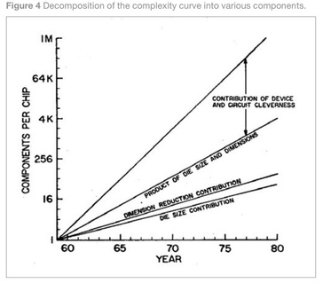
In his famous 1965 paper Cramming more components onto integrated circuits, Moore wrote: “The complexity for minimum component costs has increased at a rate of roughly a factor of two per year”. Dimensional scaling below 28nm will only increase the ‘component cost’ as described in 28nm – The Last Node of Moore's Law. |
1. “Die size”—“larger chip area”
2. “Dimension”—“higher density” and “finer geometries”
3. “Device and circuit cleverness”
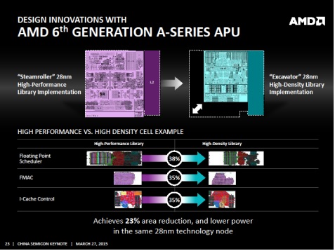
In the past, all of these factors were aggregated into dimensional scaling as old fabs got obsolete and improvements predominantly were implemented in the new emerging node. Nowadays, as dimensional scaling has reached its diminishing returns phase, we can see a very diverse adaption of technology improvments.
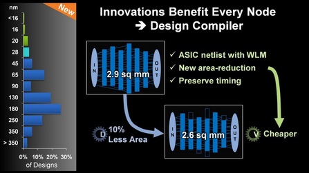
In his keynote presentation at the 2014 Synopsys user group meeting, Art De Geus, Synopsys CEO, presented multiple slides to illustrate the value of Synopsys’ newer tools to improve older node design effectiveness. The following is one of them
Finally, I’d like to quote Mark Bohr again as we reported in our blog “Intel Calls for 3D IC”: “heterogeneous integration enabled by 3D IC is an increasingly important part of scaling". This is illustrated nicely by the following figure presented by Qualcomm in their ISPD ‘15 paper titled “3D VLSI: A Scalable Integration Beyond 2D”
P.S.
A good conference to learn about these new scaling technologies is the IEEE S3S ‘15, in Sonoma, CA, on October 5th thru 8th, 2015. CEA Leti is scheduled to give an update on their CoolCube program and three leading researchers from Berkeley, Stanford and Taiwan’s NLA Lab will present their work on advanced monolithic 3D integration technologies.

Starting as soon as 2016 Qualcomm is looking to leverage Monolithic 3D IC technology to win market share in the 8 billion smartphones that will be produced from 2014 to 2018 market, said Karim Arabi, vice president of engineering at Qualcomm, speaking at the International Symposium on Physical Design (ISPD-2015, Mar. 29-April 1). This was reported by the EE Times blog titled 3D Qualcomm SoC Testing on Horizon. Arabi’s presentation slides, along with the corresponding CEA Leti slides, are now available on the ISPD-2015 conference site.
The following slide presented by Arabi illustrates their Monolithic 3D technology (“3DV”) process flow, which seem very similar to the CEA Leti CoolCube program co-sponsored by Qualcomm.
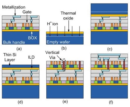
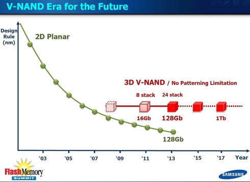
The memory industry is ramping up Monolithic 3D as we speak. 3D NAND has seen announcements from Intel, Micron and Toshiba joining Samsung. Now the logic industry is looking to adopt Monolithic 3D as we learn from this Qualcomm presentation at this ISPD-2015 and the Intel presentation at ISSCC-2015 discussed in our recent blog Intel Call’s for Monolithic 3D.
P.S.
A good conference to learn about this new scaling technology is the IEEE S3S ‘15, in Sonoma, CA, on October 5th thru 8th, 2015. CEA Leti is scheduled to give an update on their CoolCube program and three leading researchers from Berkeley, Stanford and Taiwan’s NLA Lab will present their work on advanced monolithic 3D integration technologies.

Moore’s law has swept much of the modern world along with it. Some estimates ascribe up to 40 percent of the global productivity growth achieved during the last two decades to the expansion of information and communication technologies made possible by semiconductor performance and cost improvements...
Few days later, the following chart supporting Rick’s impression was released in a new report from IHS.
The report concludes with this: "We believe that interesting years lay ahead for the semiconductor industry because the steady evolution the industry historically counted on might be coming to an end."
And it does seem that this is ahead of us as we presented in our well-read blog 28nm: The Last Node of Moore's Law.
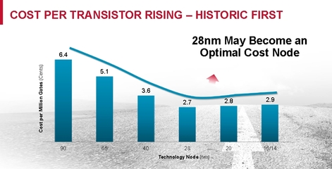
Since the publication of that blog more information has been released, mostly supporting the conclusion that 28 nm was the last node. This includes the following finding from a survey conducted by KPMG "Only a fourth of semiconductor business leaders believe Moore's Law will continue for the foreseeable future ... More than half said Moore’s Law will no longer apply at various nodes less than 22 nanometers, while 16 percent said it already has ended." Similarly, Scott McGregor, President and CEO of Broadcom, spoke at SEMI Industry Strategy Symposium (ISS) in January (Exponentially Rising Costs Will Bring Changes) and indicated that the cost per transistor was rising after the 28nm, which he described as “one of the most significant challenges we as an industry have faced.” He provided the following slide in support:
The good news is that we now have an alternative, scaling up using monolithic 3D. As was presented in last year’s IEEE S3S-2014 conference and in our blog - Precision Bonders - A Game Changer for Monolithic 3D, monolithic 3D IC could be adopted by any current fab without the need for a new recipe for transistor formation, providing very competitive costs for a wide range of product enhancements and offers a long-term road map for the industry.
- 3D InCites by Francoise von Trapp
- EDA360 Insider by Steve Leibson
- Insights From the Leading Edge by Phil Garrou
- SemiWiki by Daniel Nenni, Paul Mc Lellan, et al.
Search Blog
Meet the Bloggers
Follow us
Recommended Links
Recommended Blogs
Archives
July 2024
January 2024
December 2023
May 2023
March 2022
December 2021
August 2021
August 2018
July 2018
May 2018
October 2017
September 2017
December 2016
September 2016
August 2016
November 2015
October 2015
September 2015
July 2015
June 2015
May 2015
April 2015
March 2015
February 2015
October 2014
September 2014
August 2014
July 2014
June 2014
May 2014
April 2014
March 2014
February 2014
January 2014
December 2013
November 2013
October 2013
September 2013
August 2013
July 2013
March 2013
February 2013
January 2013
December 2012
November 2012
October 2012
August 2012
June 2012
May 2012
April 2012
March 2012
February 2012
January 2012
December 2011
November 2011
October 2011
September 2011
August 2011
July 2011
June 2011
May 2011
April 2011
March 2011
Categories
All
3d Design And Cad
3dic
3d Ic
3d Nand
3d Stacking
3d Technology
Brian Cronquist
Dean Stevens
Deepak Sekar
Dram
Education
Heat Removal And Power Delivery
Industry News
Israel Beinglass
Iulia Morariu
Iulia Tomut
Monolithic3d
Monolithic 3d
MonolithIC 3D Inc.
Monolithic 3d Inc.
Monolithic 3d Technology
Moore Law
Outsourcing
Paul Lim
Repair
Sandisk
Semiconductor
Semiconductor Business
Tsv
Zeev Wurman
Zvi Or Bach
Zvi Or-Bach

















 RSS Feed