
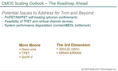
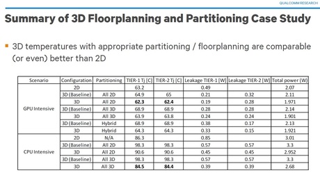
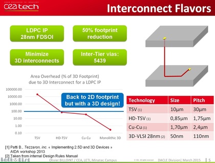
Starting as soon as 2016 Qualcomm is looking to leverage Monolithic 3D IC technology to win market share in the 8 billion smartphones that will be produced from 2014 to 2018 market, said Karim Arabi, vice president of engineering at Qualcomm, speaking at the International Symposium on Physical Design (ISPD-2015, Mar. 29-April 1). This was reported by the EE Times blog titled 3D Qualcomm SoC Testing on Horizon. Arabi’s presentation slides, along with the corresponding CEA Leti slides, are now available on the ISPD-2015 conference site.
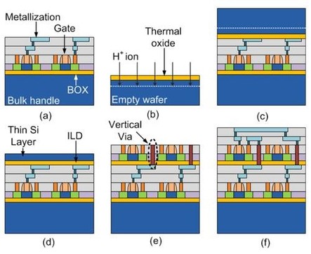
The following slide presented by Arabi illustrates their Monolithic 3D technology (“3DV”) process flow, which seem very similar to the CEA Leti CoolCube program co-sponsored by Qualcomm.
The memory industry is ramping up Monolithic 3D as we speak. 3D NAND has seen announcements from Intel, Micron and Toshiba joining Samsung. Now the logic industry is looking to adopt Monolithic 3D as we learn from this Qualcomm presentation at this ISPD-2015 and the Intel presentation at ISSCC-2015 discussed in our recent blog Intel Call’s for Monolithic 3D.
P.S.
A good conference to learn about this new scaling technology is the IEEE S3S ‘15, in Sonoma, CA, on October 5th thru 8th, 2015. CEA Leti is scheduled to give an update on their CoolCube program and three leading researchers from Berkeley, Stanford and Taiwan’s NLA Lab will present their work on advanced monolithic 3D integration technologies.



 RSS Feed