
We have a guest contribution from Zvi Or-Bach, the President and CEO of MonolithIC 3D Inc.
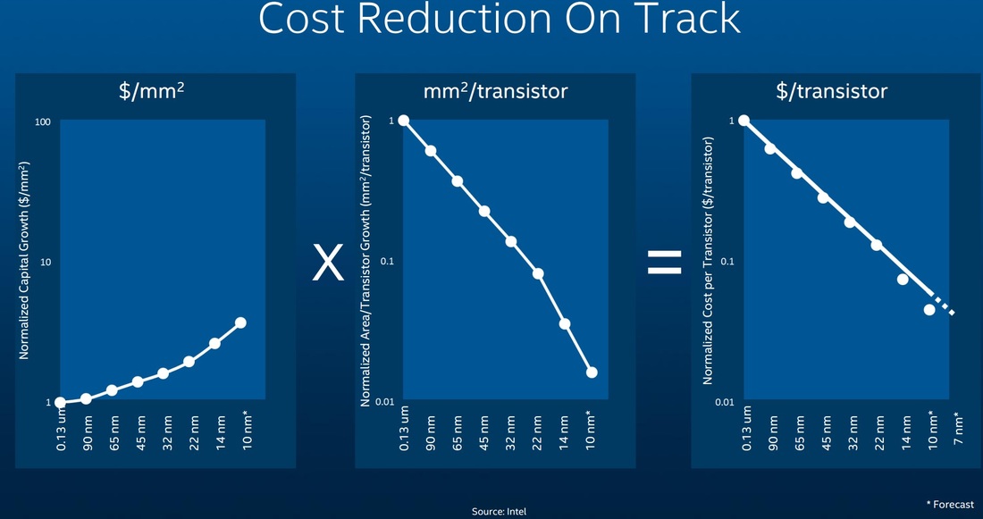
Vivek Singh, an Intel fellow, in his DAC 2015 keynote Moore's Law at 50: No End in Sight presented again the Intel chart below suggesting straight (log) line transistor cost reduction with dimensional scaling. In fact, his cost/transistor drop even seems to accelerate beyond the linear at 14 and 10 nanometers.
Vivek Singh, an Intel fellow, in his DAC 2015 keynote Moore's Law at 50: No End in Sight presented again the Intel chart below suggesting straight (log) line transistor cost reduction with dimensional scaling. In fact, his cost/transistor drop even seems to accelerate beyond the linear at 14 and 10 nanometers.
Vivek Singh, an Intel fellow, in his DAC 2015 keynote Moore's Law at 50: No End in Sight presented again the Intel chart below suggesting straight (log) line transistor cost reduction with dimensional scaling. In fact, his cost/transistor drop even seems to accelerate beyond the linear at 14 and 10 nanometers.
Less than a week later, Handel Jones (IBS) in his blog 10nm Chips Promise Lower Costs published an update down to 10nm of his well-known chart, presented below, of transistor cost with scaling.
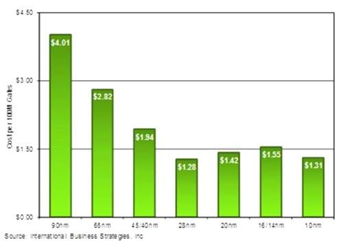
Yes, 10 nm transistor cost is a bit less than that of the 16/14nm node, but still higher than that of the 28nm node and clearly showing that the historical cost reduction of 30% per node stopped at 28nm node. From that point on Handel Jones’ cost projections have been either flat or even a bit higher. Clearly, those charts are in a striking contradiction!
The IBS chart had been supported by the other foundries and their customers, as illustrated by quotes such as the following: “Samsung spent several years developing its 14nm technology and debating which process node it would invest in after 28nm. Low expects that 28nm will still be a popular process node for years to come because of its price…The cost per transistor has increased in 14nm FinFETs and will continue to do so, …”(http://www.eetimes.com/document.asp?doc_id=1326369), “Qualcomm is looking to monolithic 3D and smart circuit architectures to make up for the loss of traditional 2D process scaling as wafer costs for advanced nodes continue to increase. .. Now, although we are still scaling down it’s not cost-economic anymore” Karim Arabi, Qualcomm VP of engineering, DAC 2014 Keynote
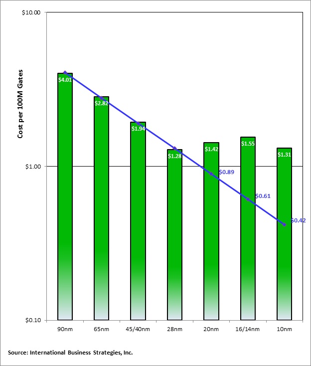
While the Intel chart Y axis has nominal values, we can plot Intel’s straight line cost reduction on the IBS chart as illustrated below on a half log scale:
The IBS chart had been supported by the other foundries and their customers, as illustrated by quotes such as the following: “Samsung spent several years developing its 14nm technology and debating which process node it would invest in after 28nm. Low expects that 28nm will still be a popular process node for years to come because of its price…The cost per transistor has increased in 14nm FinFETs and will continue to do so, …”(http://www.eetimes.com/document.asp?doc_id=1326369), “Qualcomm is looking to monolithic 3D and smart circuit architectures to make up for the loss of traditional 2D process scaling as wafer costs for advanced nodes continue to increase. .. Now, although we are still scaling down it’s not cost-economic anymore” Karim Arabi, Qualcomm VP of engineering, DAC 2014 Keynote
While the Intel chart Y axis has nominal values, we can plot Intel’s straight line cost reduction on the IBS chart as illustrated below on a half log scale:
Before jumping to our assessment of the cost difference between the green bars and Intel’s blue line, I’d like to direct you to a very detailed comment made by the “IJD” reader to Handle Jones’ blog. IJD suggests that Intel cost reduction could be explained by Intel’s very high starting point “since they effectively have a monopoly in one of the highest-margin highest volume chip markets which is x86 CPUs.”
Intel has repeatedly used their chart in effort to promote their foundry business in competition with TSMC and in the process won the Altera business. Consequently, it seems important that we should compare Intel’s costs as illustrated by the blue line vs. the green bars as reported by the rest of the industry.
We should consider the following points:
1. The Intel chart, while illustrating a simple formula, does seem logically faulty. The exponentially escalating cost of wafers needs to be neutralized by exponentially escalating scaling beyond the historical 0.7x scaling. Yet the major driver of wafer cost is lithography and it seems illogical to further reduce wafer cost by doing even more of it. Specifically, the escalating wafer cost below 28nm is driven by the need of double patterning and processing of few critical layers. Intel approach means that more layers would become critical and would need double patterning, driving the cost even higher.
2. A $0.42 per transistor vs. $1.31 per transistor should have won Intel far more foundry business, yet their major win was a very high margin vendor – Altera, and the rumor was that Altera was planning to go back to TSMC for the 10nm node. Foundry business is extremely competitive, as the customer owns the product IP and can choose the lowest cost foundry in order to win the extremely competitive end-market such as the smart phone market.
3. Intel’s $0.42 per transistor vs. the industry’s $1.31, combined with Intel’s command of the 86x CPU architecture, should have won Intel far more success in the Tablet market.
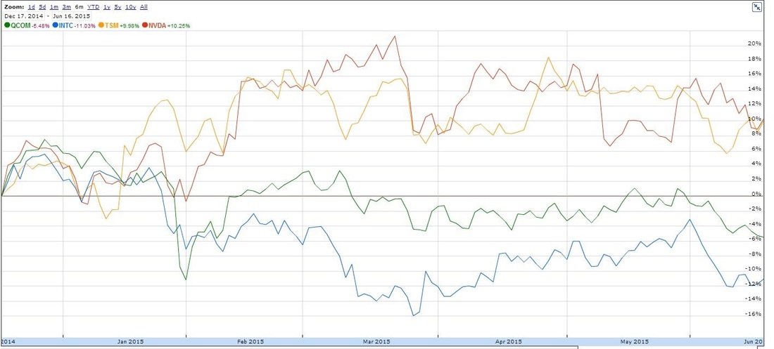
4. Looking at the last 6 months of Intel stock chart (below) in comparison to TSMC, Qualcomm and Nvidia does not show any market forecast for Intel future business resulting from its ability to beat its competitors by more than 3x the manufacturing cost.
While Intel had consistently been the process technology leader, there is no special know-how or other unique advantage that could allow Intel to have 3x better costs than its competitors.
Intel has repeatedly used their chart in effort to promote their foundry business in competition with TSMC and in the process won the Altera business. Consequently, it seems important that we should compare Intel’s costs as illustrated by the blue line vs. the green bars as reported by the rest of the industry.
We should consider the following points:
1. The Intel chart, while illustrating a simple formula, does seem logically faulty. The exponentially escalating cost of wafers needs to be neutralized by exponentially escalating scaling beyond the historical 0.7x scaling. Yet the major driver of wafer cost is lithography and it seems illogical to further reduce wafer cost by doing even more of it. Specifically, the escalating wafer cost below 28nm is driven by the need of double patterning and processing of few critical layers. Intel approach means that more layers would become critical and would need double patterning, driving the cost even higher.
2. A $0.42 per transistor vs. $1.31 per transistor should have won Intel far more foundry business, yet their major win was a very high margin vendor – Altera, and the rumor was that Altera was planning to go back to TSMC for the 10nm node. Foundry business is extremely competitive, as the customer owns the product IP and can choose the lowest cost foundry in order to win the extremely competitive end-market such as the smart phone market.
3. Intel’s $0.42 per transistor vs. the industry’s $1.31, combined with Intel’s command of the 86x CPU architecture, should have won Intel far more success in the Tablet market.
4. Looking at the last 6 months of Intel stock chart (below) in comparison to TSMC, Qualcomm and Nvidia does not show any market forecast for Intel future business resulting from its ability to beat its competitors by more than 3x the manufacturing cost.
While Intel had consistently been the process technology leader, there is no special know-how or other unique advantage that could allow Intel to have 3x better costs than its competitors.
All we can do now is watch the market evolve and eventually tell us how the gap between these widely different cost estimates will be bridged.
In any event, it is clear that Intel’s solution to the escalating cost of lithography is not sustainable. Over-scaling interconnect on its own, as Intel has sometimes hinted at, is extremely problematic because interconnect RC delays are increasing exponentially with scaling. This is nicely illustrated in the Applied Materials chart below.
In any event, it is clear that Intel’s solution to the escalating cost of lithography is not sustainable. Over-scaling interconnect on its own, as Intel has sometimes hinted at, is extremely problematic because interconnect RC delays are increasing exponentially with scaling. This is nicely illustrated in the Applied Materials chart below.
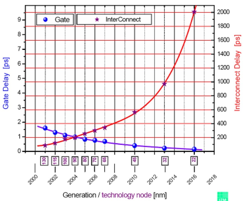
Source: B. Wu, A. Kumar, Applied Materials
The only visible solution for the coming decade is monolithic 3D. Quoting Geoffrey Yeap, VP of Technology at Qualcomm, at his invited paper at IEDM 2013: “Monolithic 3D (M3D) is an emerging integration technology poised to reduce the gap significantly between transistors and interconnect delays to extend the semiconductor roadmap way beyond the 2D scaling trajectory predicted by Moore’s Law.” And even Intel’s process guru Mark Bohr seems to have come around: “Bohr predicted that Moore's Law will not come to an abrupt halt, but will morph and evolve and go in a different direction, such as scaling density by the 3D stacking of components rather than continuing to reduce transistor size.” (http://www.v3.co.uk/v3-uk/news/2403113/intel-predicts-moores-law-to-last-another-10-years)
The only visible solution for the coming decade is monolithic 3D. Quoting Geoffrey Yeap, VP of Technology at Qualcomm, at his invited paper at IEDM 2013: “Monolithic 3D (M3D) is an emerging integration technology poised to reduce the gap significantly between transistors and interconnect delays to extend the semiconductor roadmap way beyond the 2D scaling trajectory predicted by Moore’s Law.” And even Intel’s process guru Mark Bohr seems to have come around: “Bohr predicted that Moore's Law will not come to an abrupt halt, but will morph and evolve and go in a different direction, such as scaling density by the 3D stacking of components rather than continuing to reduce transistor size.” (http://www.v3.co.uk/v3-uk/news/2403113/intel-predicts-moores-law-to-last-another-10-years)
P.S.
A good conference to learn about these new scaling technologies is the IEEE S3S ‘15, in Sonoma, CA, on October 5th thru 8th, 2015. CEA Leti is scheduled to give an update on their CoolCube program, three leading researchers from Berkeley, Stanford and Taiwan’s NLA Lab will present their work on advanced monolithic 3D integration technologies, and many other authors will be talking about their work on monolithic 3DIC and its ecosystem.
A good conference to learn about these new scaling technologies is the IEEE S3S ‘15, in Sonoma, CA, on October 5th thru 8th, 2015. CEA Leti is scheduled to give an update on their CoolCube program, three leading researchers from Berkeley, Stanford and Taiwan’s NLA Lab will present their work on advanced monolithic 3D integration technologies, and many other authors will be talking about their work on monolithic 3DIC and its ecosystem.


 RSS Feed