
We have a guest contribution from Zvi Or-Bach, the President and CEO of MonolithIC 3D Inc. Mr Or Bach presents the article published at the IEEE S3S 2014 Conference. Authors of article: Zvi Or-Bach, Brian Cronquist, Zeev Wurman, Israel Beinglass, and Albert Henning, MonolithIC 3D Inc., San Jose, CA 95124, USA.
For many years monolithic 3D was considered untenable due to the strict 400 ºC temperature limit imposed by the aluminum or copper interconnect. This led to the focus on TSV technology as the only viable path for 3D ICs. Unfortunately, it is now clear that the TSV flow in intrinsically expensive and accordingly being perpetually pushed to the future. In the recent years pioneering efforts were published providing practical paths for monolithic 3D logic devices [1-7]. But each and every one of those presented new transistor formation flows and comes along with some other non trivial process development challenges.
Recently a new wafer bonder has been introduced to the market by EVG [8]. While prior wafer bonders had about 1 micron alignment accuracy, the newly introduced Fusion Bonder has an alignment precision of 200nm (3σ). This paper proposes a process flow that leverages such precise bonder to provide a true monolithic 3D IC without the need for a new recipe for transistor formation. The process could be adapted by any current fab providing very competitive costs for a range of product enhancements and offer a long term road map for better offerings by scaling up.
Ion-Cut - A Layer Transfer Technology
The proposed flow utilizes a well-known process for single crystal thin layer transfer known as ion-cut technology. It involves hydrogen implantation, wafer bonding, and cleaving (Fig. 1). Ion-cut is a volume production qualified process that has been used for two decades in SOI wafer manufacturing. The technology was owned exclusively by Soitec for many years, which named it smart-cutÒ, but in late 2012 Soitec's fundamental patent expired and the technology is now widely available. Our estimates suggest that with re-use of substrates, ion-cut would cost less than $60 per transferred layer.
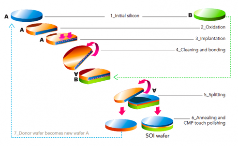
Fig. 1: Ion-Cut (smart-cut) process, stacking single crystal silicon; Soitec
Monolithic 3D IC
The following flow (Fig. 2) is built on what we call 'gate replacement' [9] and leverages the precision bonder alignment accuracy. Step 1 - a 'donor' wafer will be used to process a transistor layer labeled Stratum 3. The existing front end process could be used. Alternatively for a gate-last flow, the process will hold before the gate replacement phase. Then H+ would be implanted at the desired depth (~100nm) in preparation for the layer transfer step. Step 2 - the donor wafer is bonded (oxide to oxide) to a 'carrier wafer' and ion-cut off. This bonding step does not require precise alignment. Step 3 - the carrier wafer could be now annealed to repair the potential H+ implant damage. Step 4 - the donor wafer is now processed to form Stratum 2. The existing front line process could be used including FinFET or any other available front line process. The choice of the transistor and the architecture for Strata 2 and 3 should consider the need for vertical isolation in-between them. Note that between the transferred layer and the carrier wafer there is an oxide layer which would be an excellent etch stop allowing the transfer onto the target layer without the need for ion-cut. A preferred strategy is to use Stratum 2 for the high performance circuits while Stratum 3 would be used for support of less sensitive circuits. All high temperature should be completed at this point, as in the following step interconnects are added. Step 5 - add contacts and at least one metal layer. Step 6 - bond (oxide to oxide or metal to metal) to the target wafer using the precise bonder alignment with less than 200nm misalignment. Now grind and etch off the carrier wafer. (Not presented here are options to remove the carrier wafer for reuse.) Step 7 - the dummy gate and the gate oxide of Stratum 3 can be now replaced, and connections could be made between Stratum 2, Stratum 3 and the underneath target wafer. Alignment and via processing are just as if between conventional BEOL metal layers, as the transferred layer is very thin (~100nm).
The following flow (Fig. 2) is built on what we call 'gate replacement' [9] and leverages the precision bonder alignment accuracy. Step 1 - a 'donor' wafer will be used to process a transistor layer labeled Stratum 3. The existing front end process could be used. Alternatively for a gate-last flow, the process will hold before the gate replacement phase. Then H+ would be implanted at the desired depth (~100nm) in preparation for the layer transfer step. Step 2 - the donor wafer is bonded (oxide to oxide) to a 'carrier wafer' and ion-cut off. This bonding step does not require precise alignment. Step 3 - the carrier wafer could be now annealed to repair the potential H+ implant damage. Step 4 - the donor wafer is now processed to form Stratum 2. The existing front line process could be used including FinFET or any other available front line process. The choice of the transistor and the architecture for Strata 2 and 3 should consider the need for vertical isolation in-between them. Note that between the transferred layer and the carrier wafer there is an oxide layer which would be an excellent etch stop allowing the transfer onto the target layer without the need for ion-cut. A preferred strategy is to use Stratum 2 for the high performance circuits while Stratum 3 would be used for support of less sensitive circuits. All high temperature should be completed at this point, as in the following step interconnects are added. Step 5 - add contacts and at least one metal layer. Step 6 - bond (oxide to oxide or metal to metal) to the target wafer using the precise bonder alignment with less than 200nm misalignment. Now grind and etch off the carrier wafer. (Not presented here are options to remove the carrier wafer for reuse.) Step 7 - the dummy gate and the gate oxide of Stratum 3 can be now replaced, and connections could be made between Stratum 2, Stratum 3 and the underneath target wafer. Alignment and via processing are just as if between conventional BEOL metal layers, as the transferred layer is very thin (~100nm).
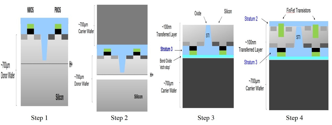
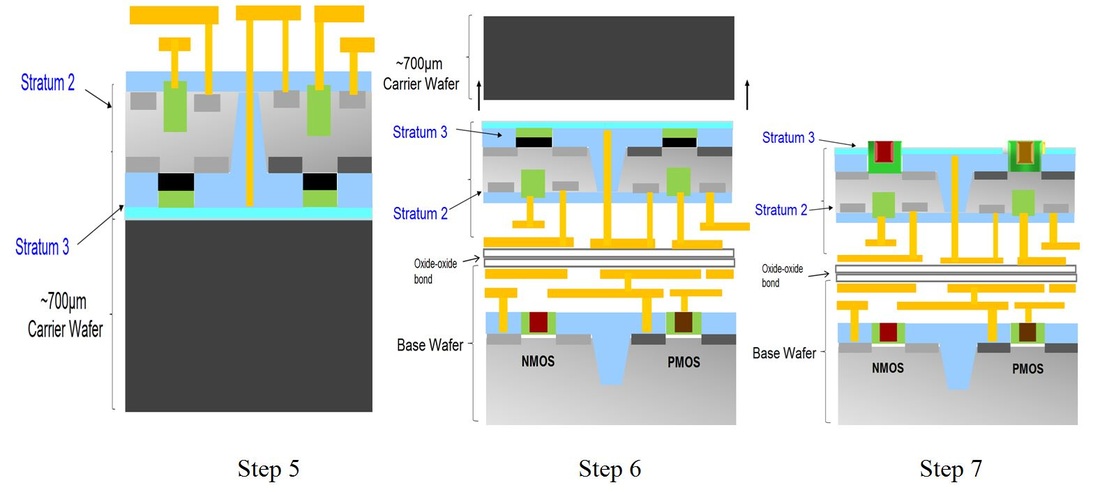
Fig. 2: Process Flow for Gate Replacement Process and precise bonding.
Smart Alignment
Having a thin transferred layer allows the through layer via to be as small as a conventional BEOL interconnection via (~50 nm). Yet the 200 nm bonding alignment window would appear to require a landing pad of 200 nm by 200nm for each vertical connection. With Smart Alignment the connection is made by two perpendicular 200 nm long strips as seen in Fig 3. The vertical strip is part of the top layer of the target (bottom) wafer. After bonding, the through layer via would be aligned to the target wafer in the X direction and to the transferred layer in the Y direction as seen in Fig 4. The top connection strip could be then processed aligned to the transferred (top) layer. This alignment scheme reduces the vertical connection overhead to minimum and allows for multiple vertical connections per unit area of 200 nm x 200 nm.
Having a thin transferred layer allows the through layer via to be as small as a conventional BEOL interconnection via (~50 nm). Yet the 200 nm bonding alignment window would appear to require a landing pad of 200 nm by 200nm for each vertical connection. With Smart Alignment the connection is made by two perpendicular 200 nm long strips as seen in Fig 3. The vertical strip is part of the top layer of the target (bottom) wafer. After bonding, the through layer via would be aligned to the target wafer in the X direction and to the transferred layer in the Y direction as seen in Fig 4. The top connection strip could be then processed aligned to the transferred (top) layer. This alignment scheme reduces the vertical connection overhead to minimum and allows for multiple vertical connections per unit area of 200 nm x 200 nm.
Fig. 3: Smart-Alignment
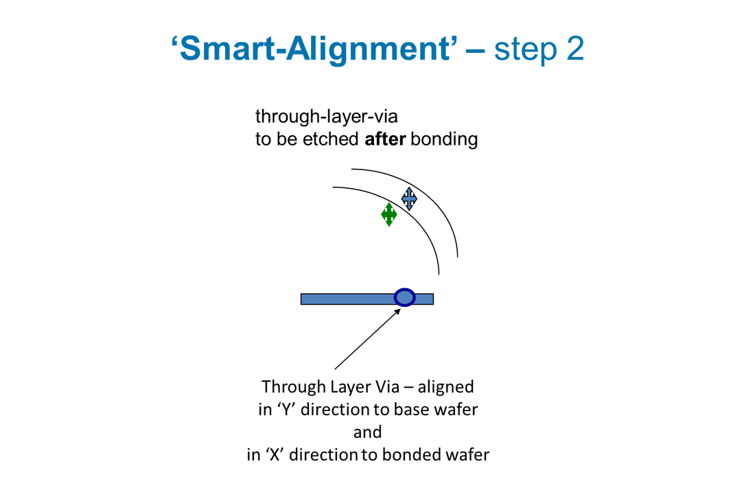
Fig. 4
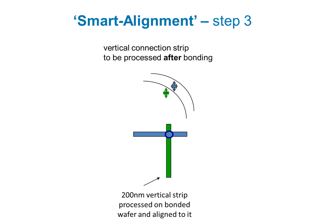
Figure 5: : Through layer via alignment

Strata 2, 3 - Examples
Fig. 5 illustrates one example for circuit allocation for Stratum 2 and Stratum 3 with an intrinsic vertical isolation. For Stratum 2, most advanced devices could be used such as FinFET transistors and forming high speed logic. The SRAM for the high speed logic circuit could be placed onto the close by Stratum 3. A compelling option for the SRAM would be the use of Zeno technology [10] where a two stable states one transistor SRAM are enabled by a deep implanted back-bias. The vertical isolation is achieved by the back-bias. The FinFET transistor by design is also isolated from the substrate. This use of Stratum 2 and Stratum 3 is compelling as there is no obstruction to the memory blockages and creates a very short path for memory access. Such dual functional layer (Stratum 2 + Stratum 3) could be a product by itself offered as an add-on to many designs and 1-chip systems. Such flows with a dual functional layer could enable many new innovative devices such as:
* An image sensor on Stratum 3 with pixel electronics on Stratum 2 could provide an unparalleled dynamic range to cameras.
* A full redundancy layer [11] as Stratum 3 provides redundancy to Stratum 2, allowing almost unlimited logic integration on huge dies, essentially a server farm on a device.
* A configurable logic fabric as an add-on...
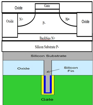
Fig 6. 1T SRAM over FinFET
Monolithic 3D Cost Estimates
It is well known that high cost is the number one issue which slows down the adoption of 3D ICs based on TSV. The proposed monolithic 3D flow has the potential to overcome these barriers as it avoids use of a thick layer with lengthy etch and deposition processes. In fact, it can provide circuit fabrics for two strata for a cost that is less than one wafer substrate. The donor wafer is reusable and the cost of the first ion-cut is estimated to be less than $60 [12]. The carrier wafer could be reusable or utilize an inexpensive test wafer costing about $30. The estimated per wafer cost of precision bonding is less than $20. Other steps involved in layer transfer, cleaning, etch, etc., are estimated at about $30 total. The costs for transistor formation for Strata 2 and 3 and their associated interconnects are no different than any other circuit fabrication costs. Accordingly we estimate that the cost structure is comparable with the fabrication cost of 2D devices. Yet having the overall design built in a 3 strata fabric provides huge power, performance, and cost benefits.
Heat Removal
A point of concern is always the heat removal aspect for 3D IC. The first question relates to having more transistors in a smaller space. While more complex circuits present an ever increasing power challenge, having it built in monolithic 3D is an important part of the solution as it is well documented [13] that 80% of the power consumption is due to on-chip connectivity. The more interesting question relates to the fact that Strata 2 and 3 transistors are thermally isolated (surrounded by oxide) and without direct access to the silicon bulk for heat removal. Fig. 6 illustrates the solution of using the power delivery network for heat removal. This work was reported in IEDM 2012 [14]. Having Stratum 2 only about 1 micron away from the bulk allows a very effective heat removal path through the power delivery network. Additional supporting techniques such as heat spreaders and thermally conducting but electrically isolated contacts could also be implemented [15].
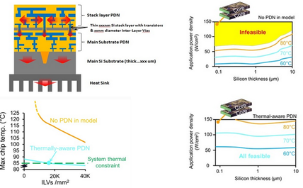
Fig. 7. Heat removal by the power delivery network (PDN) [14]
Summary
Precision Bonders combined with innovative layer transfer and alignment techniques enable a simple path to 3D IC providing the best of all worlds:
It seems that the new form of 3D IC combines the best of TSV with monolithic 3D IC to offer the most attractive path to keep Moore's Law, while opening an unparalleled path for all fabs to keep enhancing their product range using their existing equipment and flows.
And yes, this opens a new horizon for the semiconductor industry.
References
[1] Z. Or-Bach, IEEE 3DIC Conference, 2013.
[2] P. Batude et al., Proceedings of the Electro-Chemical Society (ECS) spring meeting, Vol. 16, pp.47 (2008)
[3] D. C. Sekar, IEEE 3DIC Conference, 2012.
[4] B. Rajendran, IEEE 3DIC Conference, 2013.
[5] Chih-Chao Yang 29.6 IEDM 2013
[6] Chang-Hong Shen pp. 262 IEDM 2013
[7] Sang-Yun Lee, US Patent 7,470,142
[8] Thomas Uhrmann et al., Solid State Technology, pp.14, July 2014
[9] http://www.monolithic3d.com /hkmg.html
[10] Yuniarto Widjaja US Patent 8,514,623
[11] http://www.monolithic3d.com/ultra-large-integration---redundancy-and-repair.html
[12] http://www.monolithic3d.com/blog/how-much-does-ion-cut-cost1
[13] L. Chang, IBM Short Course, IEDM 2012
[14] Hai Wei, et al., IEDM 2012
[15] D. C. Sekar US Patent 8,686,428.
Presentation:
Precision Bonders - A Game Changer for Monolithic 3D, IEEE S3S 2014, October 2014.
Precision Bonders combined with innovative layer transfer and alignment techniques enable a simple path to 3D IC providing the best of all worlds:
- Vertical connectivity density comparable with the horizontal one
- Use of existing transistor and interconnect flows
- Compatible with advanced and older fabs
- Low cost competitive with 2D IC cost structure
- Heterogonous integration - Fab lines, process nodes, device materials, processes
- Parallel and Sequential process (short TAT)
- Enables many new classes of device and systems untenable with 2D IC
- Multiple paths for cost reduction that were untenable with 2D IC
It seems that the new form of 3D IC combines the best of TSV with monolithic 3D IC to offer the most attractive path to keep Moore's Law, while opening an unparalleled path for all fabs to keep enhancing their product range using their existing equipment and flows.
And yes, this opens a new horizon for the semiconductor industry.
References
[1] Z. Or-Bach, IEEE 3DIC Conference, 2013.
[2] P. Batude et al., Proceedings of the Electro-Chemical Society (ECS) spring meeting, Vol. 16, pp.47 (2008)
[3] D. C. Sekar, IEEE 3DIC Conference, 2012.
[4] B. Rajendran, IEEE 3DIC Conference, 2013.
[5] Chih-Chao Yang 29.6 IEDM 2013
[6] Chang-Hong Shen pp. 262 IEDM 2013
[7] Sang-Yun Lee, US Patent 7,470,142
[8] Thomas Uhrmann et al., Solid State Technology, pp.14, July 2014
[9] http://www.monolithic3d.com /hkmg.html
[10] Yuniarto Widjaja US Patent 8,514,623
[11] http://www.monolithic3d.com/ultra-large-integration---redundancy-and-repair.html
[12] http://www.monolithic3d.com/blog/how-much-does-ion-cut-cost1
[13] L. Chang, IBM Short Course, IEDM 2012
[14] Hai Wei, et al., IEDM 2012
[15] D. C. Sekar US Patent 8,686,428.
Presentation:
Precision Bonders - A Game Changer for Monolithic 3D, IEEE S3S 2014, October 2014.


 RSS Feed