Monolithic 3D Inc., the Next Generation 3D-IC Company
  • Home
  • Technology
    • Technology
    • Papers, Presentations and Patents
    • Overview >
      • Background
      • Why Monolithic 3D?
      • Paths to Monolithic 3D
      • Applications
    • Ion-Cut: The Building Block
    • Monolithic 3D Logic >
      • RCAT
      • HKMG
      • Laser Annealing
      • RCJLT
      • 3D Embedded RAM
      • 3D Gate Array
      • FPGA
      • Ultra Large Integration - Redundancy and Repair
    • Monolithic 3D Memory >
      • 3D DRAM
      • 3D Resistive Memories
      • 3D Flash
    • Monolithic 3D Electro-Optics >
      • 3D Image Sensors
      • 3D Micro-Displays
  • 3D-IC Edge
    • 3D-IC Edge
  • News & Events
    • News & Events
    • S3S15 Game Change 2.0 Video/P
    • Webcast
    • Webinar
    • Press Releases
    • In the News
    • Upcoming Events
  • About Us
    • About Us
    • History
    • Team
    • Careers
    • Contact Us
  • Blog
  • Simulators

Monolithic 3D: The Most Effective Path for Future IC Scaling

4/25/2015

1 Comment

 
Webcast Overview: 

It is well recognized that dimensional scaling has reached its diminishing return phase. The industry is now looking at monolithic 3D to be the future technology driver. Yet, until recently, the path to monolithic 3D has required the development of new transistor types and processes. This Webcast will present game-changing monolithic 3D process flows, which use the existing transistor of existing manufacturing line and existing process flows. Now the most effective path for future IC scaling is indeed monolithic 3D, which offers the lowest development and manufacturing cost for future ICs.  
Download Webcast Slides
Play Webcast
1 Comment

Questions from 4/23 3D Integration Webcast

4/25/2015

0 Comments

 
1) Currently, I am working in a large project where we develop ICs and hermetic wafer level packages. My question is what are the key requirements to land on a job as a process engineer? (I hope my question is not completely out of the context)

Asked by Dilek Isik - Ecole Polytechnique de Montreal

2)Which NEMS gas sensor Technology is used by LETI?

Asked by Roberto Dossi - zmdi 

3) The benefits of 3D active on active have been clear for a while. The main feature that is missing is "AVAILABILITY" through popular manufacturing channels. Any comments on when such technology is available, say from TSMC or other known fabs at a product quality?

Asked by Alireza Kaviani - Xilinx 

A: We will be happy to post answers from anyone who knows about "AVAILABILITY"

4) Large devices such as FPGAs have many metal layers. TSVs need to go through so many of those layers to get to other active die. Are there any studies (or comments) on area overhead of such process on metal layers?

Asked by Alireza Kaviani - Xilinx

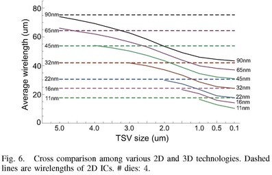
A. Studies regarding the impact of TSV do indeed show severe limitations. An advantage of monolithic 3D is that the vertical connectivity is now comparable in size with normal vias between interconnect metal layers and accordingly could highly improve circuit performance as indicated by the following chart (from IITC2011, Kim):
Picture
5) What challenges other than technical remain to be resolved before such a technology would be adopted for high volume manufactured, high performance computing products?

Asked by Jon Candelaria - Semiconductor Research Corp. 

A. "AVAILABILITY" – A vendor making monolithic 3D commercially available

6) Can you provide additional details about molecular bonding? It appears to be a critical process step for M3D.

Asked by Ajit Paranjpe - Veeco 

A. The bonding technology is now widely available and included in most cases with the bonding equipment. Ziptronix is offering their DBI bonding technology which allows reworks and other benefits. Bonding could be done oxide to oxide, metal to to metal or hybrid. Some bonding technology includes plasma treatment of the surfaces prior to bonding. 

7) How effective is molecular bonding for long term stability of he ICs? What if we need to use bonding processes with T higher than 300 C?

Asked by Dilek Isik - Ecole Polytechnique de Montreal 

A. The bonding technology is very effective. There are multiple bonding flows which could provide full bonding without the need to use temperature beyond 300 C

8) Dear Dr. Vinet, how are you doing the gate oxide of the top CMOS?

Asked by Juergen Niess - HQ-Dielectrics GmbH


9) Yield is a function of process steps. monolithic 3D has twice the number of steps (for 2 layers). Yield will be lowered as defects in any layer will kill the die. So, defect density have to be twice as good before we have the same yield. Is it likely?

Asked by TM Mak - Global Foundries 

A. Yield need to improve with any scaling. With monolithic 3D it would be easier for the following reasons:

            1. The footprint of each layer of a monolithic 3DIC is ¼ the original area, thus moving up the yield curve significantly.

            2. Since one can ‘scale’ with folding and not by shrinking, the mature process can be used, thus enjoying the previous yield ramp and incremental improvements to the yield.

            3. Heterogonous integration results in better optimization of each layer to the type of circuit it is used for.

            4. Monolithic 3D allows for a direct redundancy as presented in:
Monolithic 3D IC Could Increase Circuit Integration by 1,000x
10) What's about cost of pure stacking on Memory?

Asked by Roberto Dossi - zmdi 

A. The cost of the suggested flow is very attractive. There are no additional costs resulting from the monolithic 3D integration and the base silicon would be at reduced costs. As well, the cost of connectivity is saved altogether. Resulting with improved speed and reduced power at a lower cost.

11) Concerning the ELTRAN process: bringing so close together devices in the stratrum 2 and stratrum 3 without a thick silicon heat sink in between, how do you handle the heat generated from each layer of transistors?

Asked by Fabio Carta - Columbia University Reply 

A. The overall heat generated would be less than the same circuit on just one 2D stratum due to the shorter interconnections (CV2 and saving line buffers). Taking out the heat could be done by the Vdd and Vss lines as presented in slides #33-35. And in our blog: Can Heat Be Removed from 3D-IC Stacks?

12) 1-How does the cost multiply with the number of layers being manufactured? Is there an approximation rule for this? 2-For precise bonders, what is the cost difference between die-to-die bonding vs wafer level bonding?

Asked by Dilek Isik - Ecole Polytechnique de Montreal 

A. These are new process flow and with multiple alternatives. The rules and cost option will become clearer over time. As for the precise bonders, the presented flow is only for wafer to wafer bonding, which will have an expected cost about $20/wfr processed.

13) Have you evaluated the yield impact of the 3D monolithic approach?

Asked by Jim Wieser - Texas Instruments 

A. See 9) above

14) how can you guarantee 100nm via pitch with actual bonder alignment tolerance?

Asked by Roberto Dossi - zmdi 

A. See the section on Smart Alignment in our blog: Precision Bonders - A Game Changer for Monolithic 3D

15) What is the yield of the presented ELTRAN process?

Asked by Dilek Isik - Ecole Polytechnique de Montreal 

A. The ELTRAN process yield as was reported by Cannon and others is very high and it would have a negligible impact on the overall device yield.
0 Comments

    Author

    Write something about yourself. No need to be fancy, just an overview.

    Archives

    April 2015

    Categories

    All

    RSS Feed

© Copyright MonolithIC 3D Inc. , the Next-Generation 3D-IC Company, 2012 - All Rights Reserved, Patents Pending