
|
We have a guest contribution from Zvi Or-Bach, the President and CEO of MonolithIC 3D Inc.
This year Semicon West had a clear undertone – the roadmap forward is 3D IC. Yes, we can and we will keep pushing dimensions down, which for a few applications would be attractive, but for most designs the path forward would be “More than Moore.” |
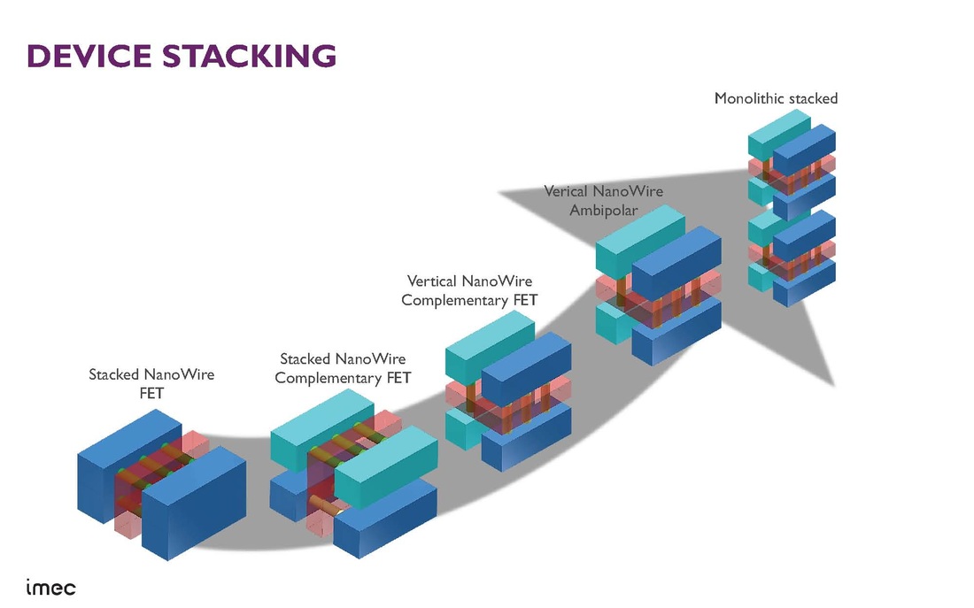
This year Semicon West had a clear undertone – the roadmap forward is 3D IC. Yes, we can and we will keep pushing dimensions down, which for a few applications would be attractive, but for most designs the path forward would be “More than Moore.” As Globalfoundries' CEO Jha recently voiced: “it's clear that More-than-Moore is now mainstream rather than niche. …Really it is leading-edge pure digital that is the niche. Instead the high-cost leading edge processes are really niche processes optimized for applications in data centers or for high computational loads, albeit niches with volumes of hundred of millions of units per year.” Similarly, EE Times editor Rick Merritt subtitled his Semicon West summary Roadmap being drawn for chip stacks. All this is nicely illustrated by the following slide presented by An Steegen of IMEC for their pre-Semicon Technology Forum:
Leti, the other major semiconductor R&D organization, has gone even further by dedicating its Semicon West day entirely to 3D technologies, as can be seen in the following invitation:
2015-LetiDay-SanFrancisco
2015-LetiDay-SanFrancisco

July 14th, 2015 W. Hotel, Social Terrace, 4th floor, San Francisco, CA. USA
GOING VERTICAL WITH LETI: Solutions to new applications using 3D technologies
- Welcome - Leti's 3D integration for tomorrow's devices > M.N Semeria
- CoolCubeTM: 3D sequential integration to maintain Moore's Law > O. Faynot
- Photonics: why 3D integration is mandatory > H. Metras
- Computing: 3D technology for better performance > S. Cheramy
- Lighting: 3D integration for cost effectiveness > I. C Robin
- Nanocharacterization for 3D > P. Bleuet
- Conclusion - Silicon Impulse > M.N Semeria

A similar view was also presented by Intel. Quoting Jeff Groff from his summary of Intel’s Q2 call: “In summary, it seems that Intel is executing fairly well on the process technology side of the business considering the ever increasing difficulty of pushing forward with Moore's Law. We can expect exciting new structures and materials (just maybe not at 10nm) and an increasing importance of 3-D structures in both logic and memory fabrication.” This echoes our blog Intel Calls for 3D IC, and was recently voiced by Intel’s process guru Mark Bohr: “Bohr predicted that Moore's Law will not come to an abrupt halt, but will morph and evolve and go in a different direction, such as scaling density by the 3D stacking of components rather than continuing to reduce transistor size.” It is also illustrated by his slide from ISSCC earlier this year.
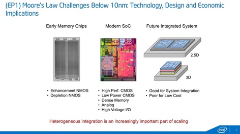
The two concerns regarding 3D IC stacking using TSV are (a) Cost, noted in the slide above “Poor for Low Cost”, and (b) Vertical connectivity, as voiced by Mark Bohr: “Intel’s Bohr agrees that 3D structures will become more important. He said the kind of through-silicon vias used for today’s chip stacks need to improve in their density by orders of magnitude.”
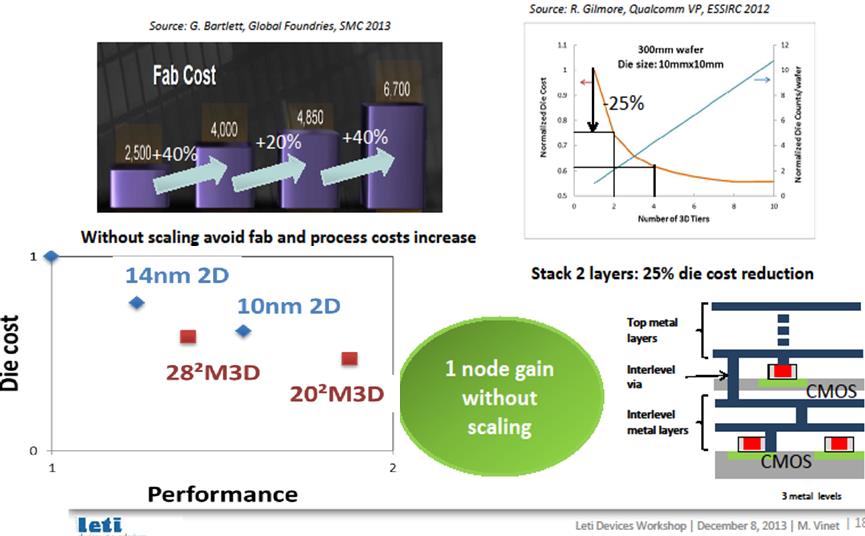
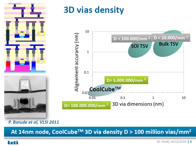
These limitations are the driver behind the efforts to develop monolithic 3D technology. Monolithic 3D would provide a very cost effective alternative to dimensional scaling with 10,000x higher than TSV vertical connectivity, as illustrated by the following two slides of CEA Leti.
These limitations are the driver behind the efforts to develop monolithic 3D technology. Monolithic 3D would provide a very cost effective alternative to dimensional scaling with 10,000x higher than TSV vertical connectivity, as illustrated by the following two slides of CEA Leti.
Prof. Subhasish Mitra of Stanford assesses a 1,000x improvement in energy efficiency using monolithic 3D. His summary at a Semicon West keynote panel: “We have an opportunity for a thousand-fold increase in energy efficiency…from collaboration between dense computing and memory elements and dense 3-D integration of them.”
While stacking using TSV does not require any change to the transistor (‘front-line’) process flow, all monolithic 3D process flows until recently required a significantly new transistor formation flow. Since the transistor process is where the majority of the R&D budget and talent is being allocated, and carries with it fresh reliability concerns, the industry has been most hesitant with respect to monolithic 3D adoption. Yet in this recent industry gathering there is a sense that industry wide interest is building up for 3D technologies. The success of 3D NAND as the first monolithic 3D industry wide adoption could help this new interest build even faster.
There is room for even more excitement. A recent technology breakthrough, first presented in IEEE S3S 2014 conference (Precision Bonders - A Game Changer for Monolithic 3D) introduced a game changer in the ease of monolithic 3D adoption. Enhancement of this breakthrough will be presented in this year’s IEEE S3S 2015. This new monolithic 3D flow allows the use of the existing fab transistor process for the fabrication of monolithic 3D devices, offering a most attractive path for the industry future scaling technology.
P.S.
A good conference to learn about these new scaling technologies is the IEEE S3S ‘15, in Sonoma, CA, on October 5th thru 8th, 2015. CEA Leti is scheduled to give an update on their CoolCube program, three leading researchers from Berkeley, Stanford and Taiwan’s NLA Lab will present their work on advanced monolithic 3D integration technologies, and many other authors will be talking about their work on monolithic 3DIC and its ecosystem.


 RSS Feed