
But other news seems different. TSMC shares are close to their historical high; Global Foundries leapfrogs TSMC technology and nips at Intel’s heels with 14nm; Samsung reports record quarterly profit. Things seem to be going swimmingly.
Semiconductor business has had its ups and downs since its inception. As demand followed, more and more capacity was put on line, which caused the next overcapacity and slump, inevitably followed by the next spike in demand as the technology inexorably marched down the scaling curve. So, perhaps, nothing is really new here after all.
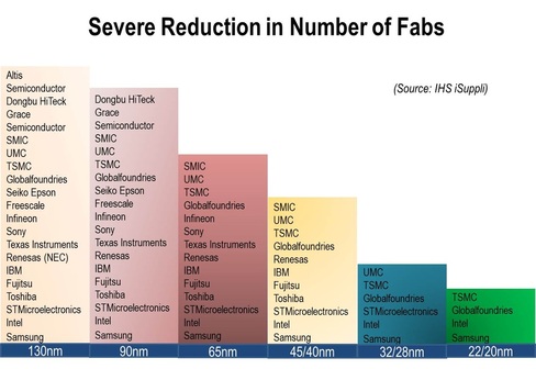
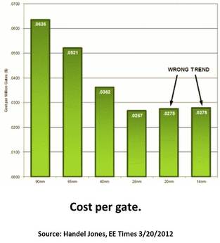
Yet, perhaps, we should not be so sanguine anymore. We did cope with 193nm light to define our chips down to 20 nm, but at an ever-increasing cost of expensive phase shift masks, immersion lithography, and double exposure. EUV has been talked about for at least 15 years (following another 15 years of x-ray lithography development fiasco) and has been “late†since at least 2005. Despite the impressive progress shown by ASML, the industry greats – Intel, Samsung, and TSMC --banding around EUV is possibly more a sign of desperation than a strong vote of confidence. The drastic reduction in foundry players – from 20 or so in 90nm to four or less for 14nm has been noticed by many and cannot be good for the long-term health and vitality of the industry.
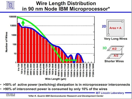
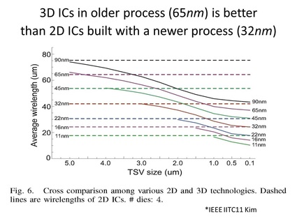
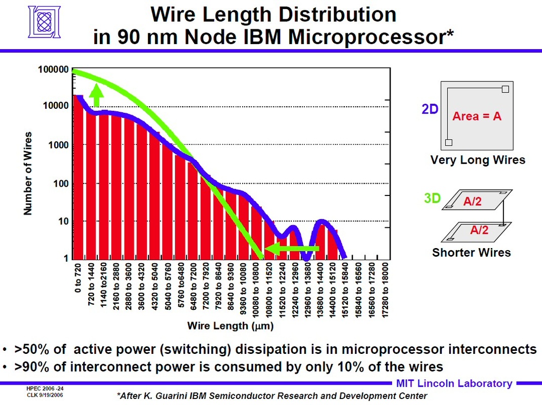
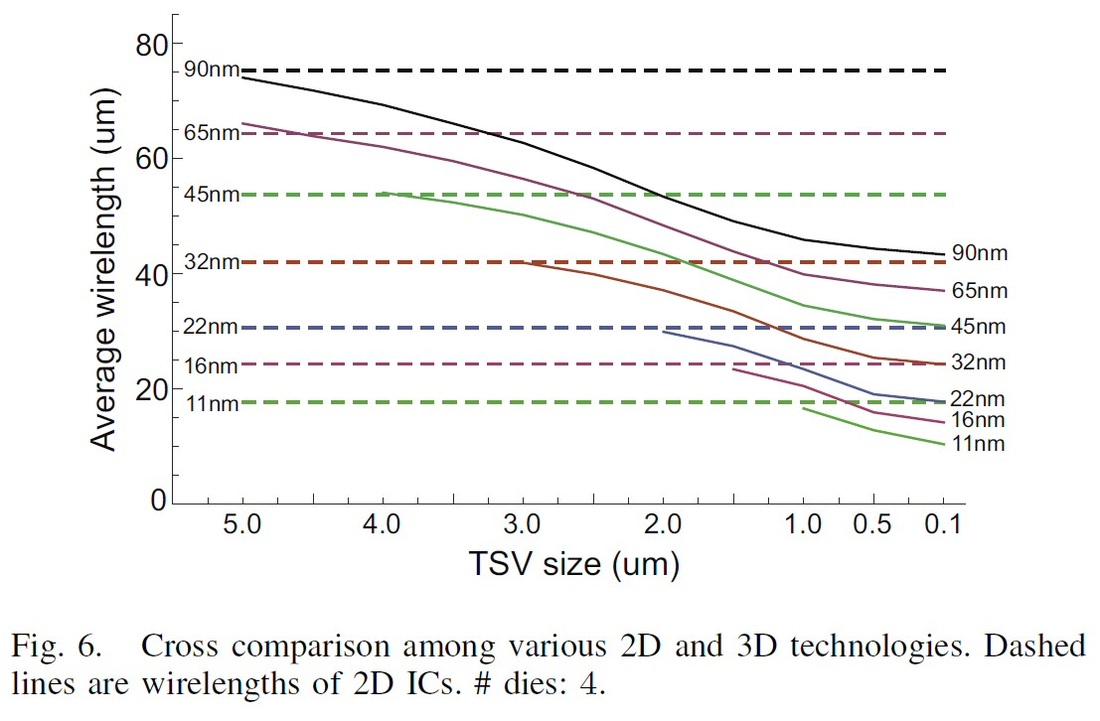
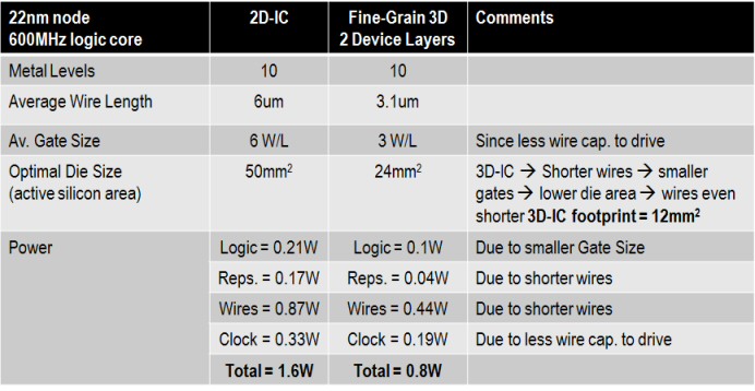
- They allow for shrinkage of the average source to destination distances, shrinking power dissipation and improving performance;
- They can include inexpensive built-in fault detection and repair as described here, allowing for as large as needed yielded dies, which cuts further on power by saving on off-chip I/O power;
- They allow cheap and high performance integration of dies with disparate technologies, so advanced (and expensive) logic can be stacked with reduced-cost technology for memory dies, or specialized analog and RF functions;
- They allow the reuse of older fab lines as much of density improvement is achieved through stacking dies rather than shrinking features;
- They allow efficient heat removal without exotic cooling technologies through use of power delivery networks, to be presented in the upcoming IEDM, paper 14.2 ;
The impact of the increased monolithic vertical integration at lower cost can be dramatic on every electronic market segment.
For mobile devices, the inexpensive integration of analog, RF, and sensors, can lower their cost and power consumption for an even broader market penetration and longer battery life.
In medicine, the footprint of devices is often critical. The availability of camera-in-a-pill, or of implantable medical devices that control drug release, improve hearing, monitor vital signs, or allow artificial vision, are all strongly dependent on heterogeneous device integration in a small footprint and with reduced power. Monolithic 3D is key to transforming the planar and bulky designs of today’s 2D to grain-of-corn and grain-of-rice shape factors that can be inserted for very long time periods into our bodies.
Fostering innovation and reducing barriers to entry of new products are considered crucial for future economic prosperity. FPGAs have been trying to fill this niche since the demise of ASICs, yet they suffer from many handicaps: they are physically large, they are power hungry, and they are available in a limited number of configurations that are often suboptimal for the application. Monolithic 3D technology allows the inexpensive creation of a nearly infinite number of FPGA configurations that can be tailored to every application, as described here. And it does so while dramatically reducing both the device footprint and power.
Large-scale computing is facing enormous challenges to reduce its power consumption. Server farms of the likes of Google, Amazon, or Facebook consume tens and hundreds of megawatts of energy, while the government struggles mightily to keep its planned Exascale supercomputer under 20MW. Three-dimensional chips can play a large role in reducing power consumption by reducing the interconnect length (and hence, its capacitance), which is responsible for most of the power dissipation in modern chips. Ultra large scale integration with high yields, enabled through 3D repair structures, will further slash the power that today resides in the off-chip drivers.
In memory design, the transition to 3D technology is already taking place as described in our previous blog. Monolithic 3D structures using crystalline silicon may further the penetration and efficacy of this technology in both non-volatile memory as well as in DRAM.
The semiconductor world will inevitably move to monolithic three-dimensional technologies. The change drivers are already here: the skyrocketing cost of scaled-down lithography, the need to reduce power dissipation, and the need for heterogeneous integration. The only question is how quickly it will move there, and who will be the winners.





 RSS Feed