
We have a guest contribution today from Ze'ev Wurman, MonolithIC 3D Inc.'s Chief Software Architect. Ze'ev discusses yield and repair issues with 3D stacked chips.
Last month we described how monolithic 3D layers enable super large scale integration using redundancy layers. In that approach each logic layer is duplicated and adding a regular symmetric vertical connectivity between these layers allows swapping in a replacement logic cone for each faulty logic cone on the main layer. This permits close to 100% yield for arbitrary-sized chips, up to wafer-scale size, at the cost of dedicating a repair layer for each logic layer.
Today I will describe an alternative method that addresses the repair of multiple stacked layers of logic by a single stacked repair layer. Like before, this method offers close to 100% yield and enables super large scale integration devices up to a wafer size.
Today I will describe an alternative method that addresses the repair of multiple stacked layers of logic by a single stacked repair layer. Like before, this method offers close to 100% yield and enables super large scale integration devices up to a wafer size.
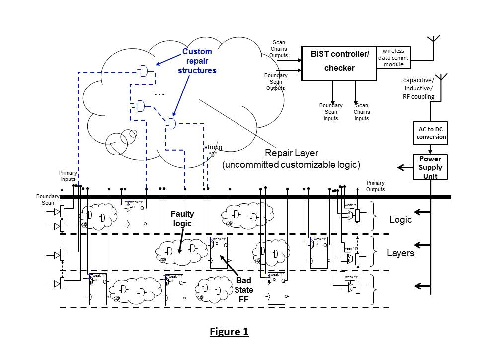
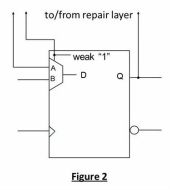
The principle behind this method is quite simple and relies on the dense vertical connectivity offered by monolithic 3D technology, as well as the inexpensive availability of direct-write e-beam lithography. (The word “inexpensive” in the previous sentence is not a typo.) Figure 1 provides an overall view of this approach. It consists of N stacked layers of logic, with an N+1 repair layer on top. The logic is conventionally scan-based, but uses a special flip flop that has an additional multiplexer in front of the FF input, as described in figure 2. By default, this mux is steering the regular logic input into the flop through a weak pullup at its control. The additional mux input and its control are vertically routed to the repair layer, which also has the output of the flop available. We should observe that having three vertical connections for every flop, and at multiple logic layers, can be easily achieved with monolithic 3D but is not feasible for most designs with TSVs – they are simply too big.
The repair flow is pretty straightforward. The wafer is completed through its N layers of logic and half-way into the top repair layer, up to its metal 3 or 4. At that point the BIST controller and the contactless data communication and power harvesting modules should be completed (more on them later). Scan testing is performed using this contactless powering and probing and the on-board BIST controller, and any failing logic cones are identified. External CAD software then synthesizes the failing logic cones in the repair layer using the flop outputs available there, and places them in a close proximity to the original x,y location of the logic – except that on the repair layer -- to maintain timing similar to the original one. Output of the synthesized replacement logic is fed to the appropriate flop mux input, and the mux control is tied to logic 0 to steer this replacement logic to the flop. This is depicted by the blue repair structures in figure 1.
The repair layer can be made of a gate-array-like terrain, or of some other metal-programmable type of terrain. An important element is that this terrain needs to be routable (and programmable, if need be) using a small number of metal segments on a single metal layer or, ideally, only metal vias on a single via layer. Similar segmented routing fabrics are routinely used by FPGA companies and by structured ASIC manufacturers such as ChipX and eASIC. With such segmented metal fabric, the e-beam machine needs to spend minimal time – a matter of minutes per wafer – to implement the repair structures on the repair layer. After that step, the fabrication of the wafer continues to completion, except that now each chip-site/die has a customized repair structure in place.
A few points are worth noting. First, since the vertical distance added by each layer is on the order of a micron, the distances (and timing) are essentially preserved when using the repair layer. Further, the transistors on the repair layer can be made somewhat faster (and more power hungry) than the logic layer transistors, as only a handful of the repair transistors will ever be actually used; hence their impact on the overall power dissipation is miniscule. Second, in a typical manufacturing flow one expects faults on the order of one per square centimeter or less and, even with multiple stacked layers, a single repair layer contains plenty of transistors available to effect repairs of a few logic cones at this fault density. Third, it should be noted that this particular approach does not address the case when the fault is in the flop itself. Flops typically occupy only a fraction of the silicon area and the impact of this restriction on yield is minimal.
One may wonder how realistic the contactless approach to testing wafers is. Just last month ST Microelectronics announced first commercial wafer-level contactless testing. At the 2011 ISSCC, Keio University (Yokohama, Japan) researchers announced inductive harvesting of 6 watts of energy with a 5x5 mm square chip. A year before that they demonstrated a 6 Gb/s wireless transfer rate per pin with a 300x300 micron antenna size, and in 2009 a group from the same university demonstrated contactless probing that can perform DC measurement. (The links require IEEE subscription). Clearly, contactless testing is coming just in time to assist with the testing of large 3D chips.


 RSS Feed