
We have a blog post today from Ze'ev Wurman, the Chief Software Architect of MonolithIC 3D Inc. Ze'ev spent many years leading EDA/software work at Dynachip, eASIC and Amdahl. In today's post, he explores vertical integration in the world of FPGAs.
Rapid escalation of access price to cutting edge technology decimated the number of ASIC designs since 2000, and directed much attention to FPGAs as ASICs replacement. Yet, despite more than a decade of predictions that FPGAs will take over the semiconductor world, this has not happened. In 2000 the FPGA market stood at less than $4B, or about 2% of the total semiconductor market, and last year it was less than $5B or only about 1.5% of the total marker. Clearly, FPGAs did not conquer the (semiconductor) world.The reasons are pretty obvious. Despite their impressive advances in speed and density, FPGAs are still 20 or more times less dense than corresponding ASICs (PDF), 10 times more power hungry, and at least twice slower. Sure, there are exceptions to these for some applications, but overall the picture is not very encouraging. Since much of their disadvantages stem from the area penalty of the programmable interconnect that blows up the die size—and the corresponding power dissipation and delay, efforts have been made to take advantage of three-dimensional stacking to reduce those distance-related penalties.
Tier Logic placed the configuration memory as a second-tier TFT layer. Lin and El Gamal from Stanford explored three-dimensional architectural FPGA variants (PDF) such as in figure 1 and found potential area reduction of up to a factor of 3.2, with concomitant reduction of power and delay by up to 1.7. Le, Reda and Behar from Brown University suggested 3D architectural partitioning across block types (PDF), such as relocating large user memories or DSP blocks to other tiers, and finding smaller potential improvements. Yet the big issue with all these ideas is the fact that nobody knows how to manufacture them: even with state of the art TSVs the vertical connectivity demands are overwhelming, while Tier Logic found that it could not resolve the reliability problems associated with TFT devices.
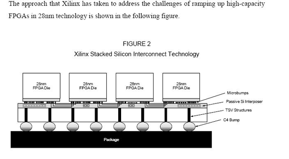
Recently Xilinx came up with a hybrid solution that placed multiple FPGA dies on a passive silicon interposer that connects among the logic of the FPGA dies (fig. 2). Xilinx claims large power savings by avoiding the need for full-sized off-chip drivers for the short signals on the interposer, yet, at best, this is a half-way measure rather than anything close to a true 3D IC architecture.
Finally, there is a matter of development cost. Coming out every couple of years with a new device family, with the cost to design and tapeout a dozen or more family members, while porting all the IO, PLLs and SerDes to a new technology is not a cheap operation and must cost in the hundreds of millions. Xilinx and Altera have invested years in this process and even they barely have the resources to execute it over and over again with ever-increasing technology costs. Something will have to give.
An effective three-dimensional FPGA solution will address two key issues: it will provide a solution that will take advantage of the third dimension to significantly reduce the average distances between circuits that will result in a large decrease in power dissipation and increase in performance; and it will provide a manufacturing solution so that building these device will be less expensive, and allow the reuse of older-generation analog and quasi-analog elements, which do not need to track the inexorable march of logic technology, such as IOs.
We believe we have a good solution to this problem, which we will present in the near future.
Tier Logic placed the configuration memory as a second-tier TFT layer. Lin and El Gamal from Stanford explored three-dimensional architectural FPGA variants (PDF) such as in figure 1 and found potential area reduction of up to a factor of 3.2, with concomitant reduction of power and delay by up to 1.7. Le, Reda and Behar from Brown University suggested 3D architectural partitioning across block types (PDF), such as relocating large user memories or DSP blocks to other tiers, and finding smaller potential improvements. Yet the big issue with all these ideas is the fact that nobody knows how to manufacture them: even with state of the art TSVs the vertical connectivity demands are overwhelming, while Tier Logic found that it could not resolve the reliability problems associated with TFT devices.
Recently Xilinx came up with a hybrid solution that placed multiple FPGA dies on a passive silicon interposer that connects among the logic of the FPGA dies (fig. 2). Xilinx claims large power savings by avoiding the need for full-sized off-chip drivers for the short signals on the interposer, yet, at best, this is a half-way measure rather than anything close to a true 3D IC architecture.
Finally, there is a matter of development cost. Coming out every couple of years with a new device family, with the cost to design and tapeout a dozen or more family members, while porting all the IO, PLLs and SerDes to a new technology is not a cheap operation and must cost in the hundreds of millions. Xilinx and Altera have invested years in this process and even they barely have the resources to execute it over and over again with ever-increasing technology costs. Something will have to give.
An effective three-dimensional FPGA solution will address two key issues: it will provide a solution that will take advantage of the third dimension to significantly reduce the average distances between circuits that will result in a large decrease in power dissipation and increase in performance; and it will provide a manufacturing solution so that building these device will be less expensive, and allow the reuse of older-generation analog and quasi-analog elements, which do not need to track the inexorable march of logic technology, such as IOs.
We believe we have a good solution to this problem, which we will present in the near future.
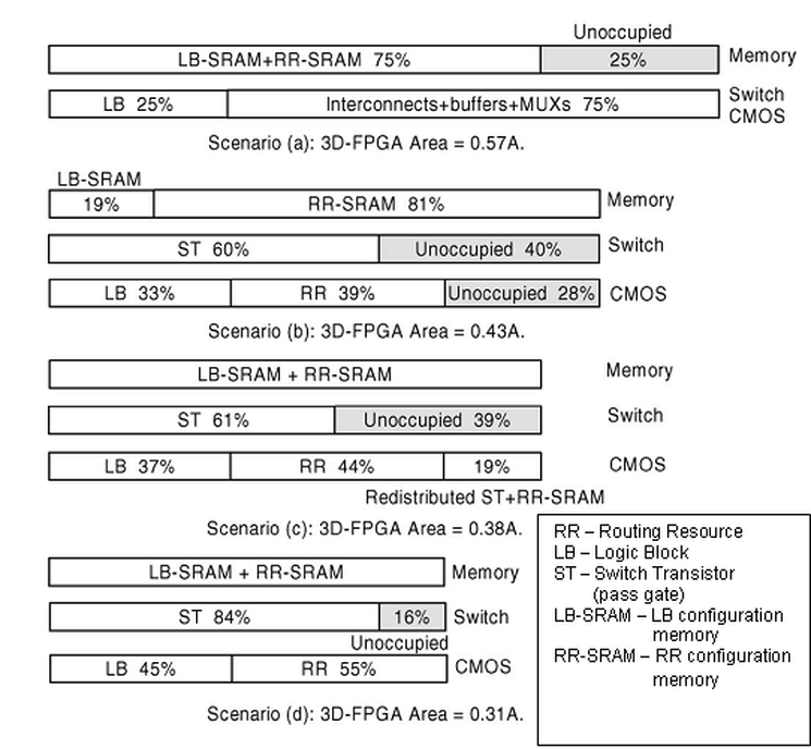
Figure 1: 3D FPGA, Lin & El Gamal, 2007.


 RSS Feed