
We have a guest contribution today from Ze'ev Wurman, the Chief Software Architect at MonolithIC 3D Inc. Ze'ev discusses some interesting implications of 3D technology for FPGAs.
Last time we discussed three-dimensional FPGAs, it became clear that there are two major areas that block wider acceptance of current 2D FPGAs: their relative inefficiency in area (i.e., cost) power and performance as compared to ASICs, and the limited number of sizes that are offered by vendors due to the high cost associated with each family member.
The advantage of going to 3D was also discussed. Architectures such as suggested by Lin and El Gamal from Stanford, and by Le, Reda and Behar from Brown promise to reduce the footprint of a three dimensional stack by a factor of 3 or more, resulting in long wire distance reduction of more than 40%. Experiments show that also the average wire length is reduced in such cases. As we know, the majority of dynamic power dissipation in deep submicron designs resides in the interconnect power, so a shorter average wire length will directly reduce the power of such three-dimensional FPGAs. Simultaneously, the shorter long wires will also increase the FPGA performance.
But such architectures require dense vertical connectivity between device layers that TSVs cannot provide. Only now, with the true monolithic 3D technology we bring to the market, this dream may be realized.
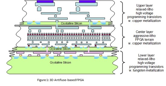
And the story just gets better. Antifuse-based FPGAs have been on the market for many years, but their efficiency was always hampered by the large, high-voltage, programming transistors that needed to share the terrain with the logic block. Three dimensional FPGAs allow designing highly effective antifuse-based FPGAs, where the high voltage programming transistors reside in layers above and below the FPGA fabric itself. Antifuses can be as small as regular vias and allow for a much better programmable connectivity as compared to SRAM-based FPGAs. This arrangement is shown in Figure 1, with antifuses marked in red. An added advantage of the two layers of programming transistors above and below the FPGA is that the one below can program the CLB, while the one above can program the interconnect. Thus each programming path does not have to unnecessarily cross multiple metal layers and increase routing congestion.
The advantage of going to 3D was also discussed. Architectures such as suggested by Lin and El Gamal from Stanford, and by Le, Reda and Behar from Brown promise to reduce the footprint of a three dimensional stack by a factor of 3 or more, resulting in long wire distance reduction of more than 40%. Experiments show that also the average wire length is reduced in such cases. As we know, the majority of dynamic power dissipation in deep submicron designs resides in the interconnect power, so a shorter average wire length will directly reduce the power of such three-dimensional FPGAs. Simultaneously, the shorter long wires will also increase the FPGA performance.
But such architectures require dense vertical connectivity between device layers that TSVs cannot provide. Only now, with the true monolithic 3D technology we bring to the market, this dream may be realized.
And the story just gets better. Antifuse-based FPGAs have been on the market for many years, but their efficiency was always hampered by the large, high-voltage, programming transistors that needed to share the terrain with the logic block. Three dimensional FPGAs allow designing highly effective antifuse-based FPGAs, where the high voltage programming transistors reside in layers above and below the FPGA fabric itself. Antifuses can be as small as regular vias and allow for a much better programmable connectivity as compared to SRAM-based FPGAs. This arrangement is shown in Figure 1, with antifuses marked in red. An added advantage of the two layers of programming transistors above and below the FPGA is that the one below can program the CLB, while the one above can program the interconnect. Thus each programming path does not have to unnecessarily cross multiple metal layers and increase routing congestion.
Flexible manufacturing
As mentioned before, the cost of designing each member of an FPGA family is very high, and the cost of the whole family is prohibitive. Even Xilinx and Altera struggle with the huge R&D expenditure every other year to follow the technology curve. Yet, despite this huge investment by the vendors, most customers eventually have to pay for chips that are typically 20% bigger than actually necessary for their designs. Not only that, but each such chips will carry many additional elements that are not fully utilized – be it multipliers, SerDes circuits, memory blocks, or I/O pins.
Imagine instead if a whole wafer of an FPGA was dedicated to its logic fabric, but without any I/O. Every so often this terrain would be interrupted by a gap of perhaps 100 microns, with only long tracks crossing perpendicularly across that gap. This is a concept known as Continuous Array, and is illustrated in Figure 2.
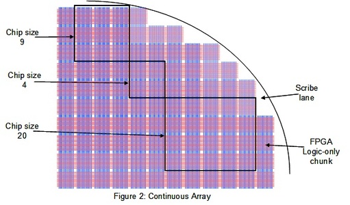
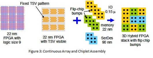
The gaps between the “logic chunks” of FPGA terrain serve as potential scribe lanes, and based on customer demand the wafer can be diced in a variety of sizes. The top metal layer of the Continuous Array has a TSV (or microbump) prepared in a regular pattern, connected to the programmable interconnect. Now imagine that we design “chiplets” of I/O, SerDes, block memory and similar, each chiplet being of the exact physical size of the FPGA terrain logic chunk, with corresponding TSV (or microbump) pattern below, and with flip-chip bumping on its top. A customer can then specify the size of the logic needed for his design, and the type of chiplets needed to complete the design – how many I/Os, how much block memory, and how many SerDes macros. As can be seen in Figure 3, an almost infinite variety of configurations is possible with just a handful of mask sets.
Yet another advantage of this configuration is that one can reuse chiplets from an older technology over multiple generations of FPGA products. This makes it much easier to come to the market with pre-qualified IO from previous products without the tedious and difficult process of re-certification.
As we see, there are many options and savings that open up with monolithic 3D integration. For example, one can imagine a stack of single or multiple monolithic block memory layers on top of FPGA logic, topped with variety of IO chiplets, to offer a wider range of logic to memory ratios than currently available today.
As we see, there are many options and savings that open up with monolithic 3D integration. For example, one can imagine a stack of single or multiple monolithic block memory layers on top of FPGA logic, topped with variety of IO chiplets, to offer a wider range of logic to memory ratios than currently available today.


 RSS Feed