
We have a guest contribution today from Ze'ev Wurman, MonolithIC 3D Inc.'s Chief Software Architect. Ze'ev discusses yield issues with 3D stacked chips.
When the subject of vertical stacking of active layers is discussed, the question of yield comes up frequently. We all know that chips have defects – after all, that’s the main reason why Xilinx chose to offer their large 28nm FPGAs as stacked dies on an interposer instead of simply making a larger chip. But when one stacks one aggressive litho die on top another – or worse yet, four or six on top of each other – surely the aggregate yield of this expensive stack must plummet, right?
Turns out that such simplistic approach does not have to be right. In fact, we will see that a clever use of monolithic stacking allows us to increase the yield, and reliably manufacture much bigger devices than previously possible.
The basic idea behind yield improvement in monolithic 3D is the concept of repair. We are familiar with this concept from big memory arrays, where we create spare rows or columns, and switch them in as needed using some form of programming to replace faulty memory elements. This works for memory arrays because they are designed to have uniform access time across the whole array, and replacing one column by another that is physically located elsewhere makes no functional difference. In logic terrain, however, this is effectively impossible. Many logic paths are finely tuned and have little slack. Replacing a faulty element in such path with another, which may be far away from the location of the original element, is bound to fail because of the additional delay that is introduced.
This picture changes with monolithic 3D design. We can design our logic on N layers, and we can then place an additional (N+1) layer on top of the stack, dedicated to the repair of the layers below. One example of such architecture is schematically depicted below.
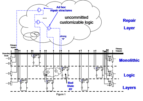
With the dense vertical connectivity that monolithic stacking offers, we can bring the output of every flop to the top repair layer, and we can multiplex an additional input to every flop from that layer. The repair layer itself consists of uncommitted logic that can be programmed late in the manufacturing process through, for example, direct-write e-beam machine. Using this technique we can create large number of ad-hoc repair structures as needed, based on the diagnosed faults in the lower N layers. The beauty of this architecture is that one can create the repair structure right above the fault, and with each monolithic layer being perhaps only 1-2 microns thick, the replacement delay will be similar to the delay of the original logic. One can even make the repair layer of ultra fast (and power hungry) logic to provide additional timing margin, as only a tiny fraction of that repair layer is ever used. A true “drop in” replacement!
We have described here one repair architecture, but others are possible. The key point to remember is that with multi-layer stacking we can afford to have silicon dedicated to repair right above where any potential logic fault can occur.
Before I finish this post, let me touch on another intriguing possibility. Thirty years ago Gene Amdahl gave up on his dream of wafer-scale integration, when he realized that the yields needed for a wafer-scale device will not be attainable for perhaps another 100 years. Yet monolithic 3D stacking with a repair layer brings Amdahl’s dream within our reach. After all, with a repair capability on a logic cone-by-cone basis, nothing stops us from achieving close to 100% yield even at the level of a full wafer.


 RSS Feed