The next International Interconnect Technology Conference (IITC 2012) will be held in San Jose in a couple of weeks (June 4-6). This is a good opportunity to recall that, in some sense, the reason for scaling silicon down has changed in recent years from packing more transistors in a square (or cubic) millimeter to increasing functionality and performance at reduced power. An ever higher fraction of the power dissipation resides in the interconnect – both in the net switching itself as well as in the ever-increasing number of repeaters required to re-power more and more “long†nets.
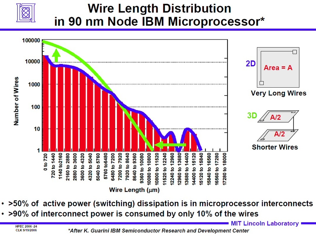
Estimates of the area dedicated to repeaters as technology shrinks vary but even if the early predictions of 70% cells being dedicated to repeaters at 32 nm may have not come to pass (Saxena, TCAD 2004), a large fraction of chip power is now dissipated by interconnect structures. This is particularly true in FPGAs where the interconnect share of routing-related dynamic power may easily reach 2/3 of the power, but even non-programmable devices have been reported to have half of their power dissipated in the wires already at 90nm. The following slide is from the 2006 High Performance Embedded Computing workshop.
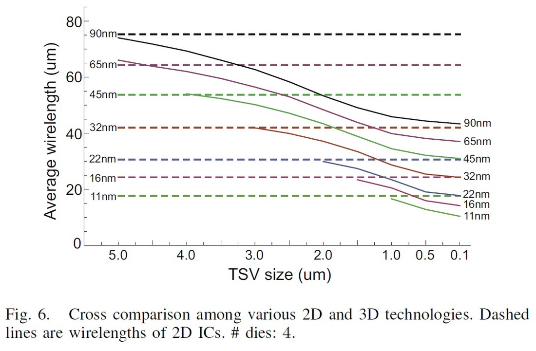
Yet there is a fly in this ointment – TSVs with aspect ratio of 50:1 are not likely to happen, and using nanometer-TSV with extremely thin silicon layers to maintain AR below 10 creates problems of its own. Just recently IMEC reported stress issues at 25 micron thickness and “found that increase in the die thickness from 25 to 50 um resulted in a stress reduction of 3X. Final conclusions were that 50 um thickness die were currently much better option for scalable manufacturable process.†In other words, the road to nanometer-scale vertical connections does not go through scaling down TSVs but through monolithic process and layer transfer.
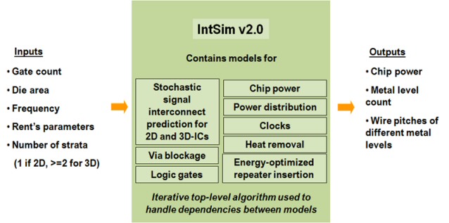
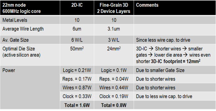
I find all this a nice illustration of the importance of the monolithic stacking approach that is also easily visible using our free simulator, IntSim.


 RSS Feed