Monolithic 3D Inc., the Next Generation 3D-IC Company
  • Home
  • Technology
    • Technology
    • Papers, Presentations and Patents
    • Overview >
      • Background
      • Why Monolithic 3D?
      • Paths to Monolithic 3D
      • Applications
    • Ion-Cut: The Building Block
    • Monolithic 3D Logic >
      • RCAT
      • HKMG
      • Laser Annealing
      • RCJLT
      • 3D Embedded RAM
      • 3D Gate Array
      • FPGA
      • Ultra Large Integration - Redundancy and Repair
    • Monolithic 3D Memory >
      • 3D DRAM
      • 3D Resistive Memories
      • 3D Flash
    • Monolithic 3D Electro-Optics >
      • 3D Image Sensors
      • 3D Micro-Displays
  • 3D-IC Edge
    • 3D-IC Edge
  • News & Events
    • News & Events
    • S3S15 Game Change 2.0 Video/P
    • Webcast
    • Webinar
    • Press Releases
    • In the News
    • Upcoming Events
  • About Us
    • About Us
    • History
    • Team
    • Careers
    • Contact Us
  • Blog
  • Simulators

Paradigm Shift in Semiconductor Industry

9/4/2014

0 Comments


28nm: Clearly the Last Node of Moore's Law for Most Designs

Picture
We have a guest contribution from Zvi Or-Bach, the President and CEO of MonolithIC 3D Inc. Mr. Or-Bach discusses about the paradigm shift in the semiconductor industry. 

In our blog 28nm – The Last Node of Moore's Law, we had pointed out that the change has happened, and it is no longer a matter of forecast or prediction. In this blog we will start by reviewing some of what has transpired since that blog, and then focus on the ensuing paradigm shift in the semiconductor industry.

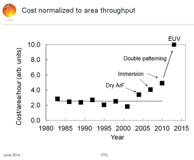
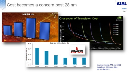
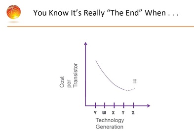
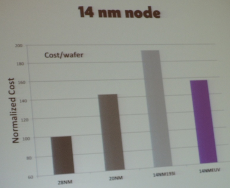
The following chart was presented in the IEEE IITC workshop by Globalfoundries. It illustrates the cost impact of the double patterning required for scaling below 28/22 nm. 
Picture
Soon after Rick Merritt’s coverage of Semicon West - 13 Things I Heard at Semicon West -- Rick wrote: "Moore's Law has definitely slowed" quoting Gartner semiconductor analyst Bob Johnson."No matter what Intel says, Moore's Law is slowing down" and, Bob added, "Only a few high-volume, high-performance apps can justify 20 nm and beyond."

Soon thereafter Peter Singer, in a blog post about the ConFab 2014 –  Can we take cost out of technology scaling? -- quotes Dr. Gary Patton, VP of semiconductor research and development center at IBM: “The challenge we’re facing now is two fold. Number one, we’re struggling to get that 0.7X linear scaling. It might be about 0.8X. And we’re adding a lot more complexity, especially when you adding double and triple patterning."

And now, in early August we finaly got more information from Intel about their up coming 14nm. In our blog Intel vs. Intel we articulate that Intel’s numbers indicate that Moore’s Law had stopped at 28/22 nm both in terms of the bring-up time it takes and the cost of new technology nodes.

It is hard to accept that a trend that has held strong for 50 years, and which kept going many years after multiple predictions of its imminent demise, has really stopped. And it is even harder as we watch the huge effort of bringing up the 14 nm and 10 nm nodes. Yet it seems that everybody should agree that the semiconductor industry is now going through a paradigm shift and for most designs 28nm is, at least for some time, the last node of Moore's Law.

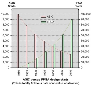
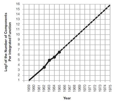
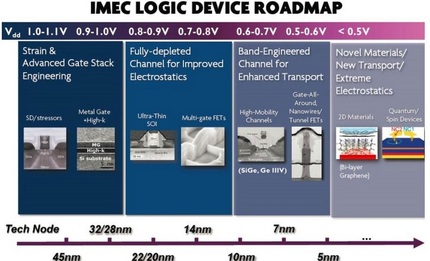
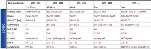
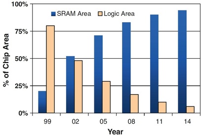
The following charts are well known and present the reason for that change.


Picture
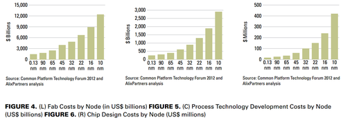
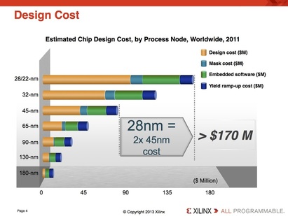
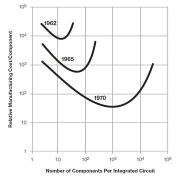
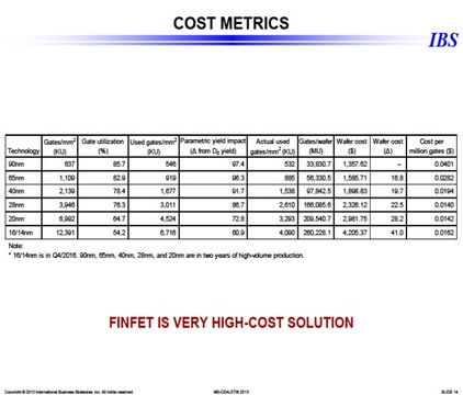
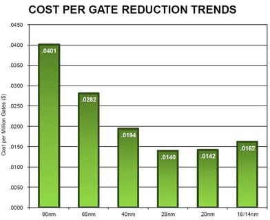
It shows that the design cost increases by more than $100M from 32nm to 16nm. If we assume a die cost of $10 at 32 nm and we assume that the traditional cost reduction per node still holds, then we would need a volume of more than 20 million units just to break even. If one also considers the risk associated which such a design, it would actually require more than 100 million units, or at least $1B of market, for such device to justify the investment. Clearly, very few designs have the market for 100 million units or $1B market.
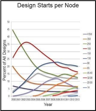
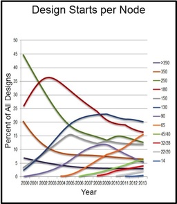
The following chart by IBS presents the past trend in design starts per node. Clearly, most new designs are still done in 130 nm while the node with the fastest ramp-up is 65 nm.

Picture
The forcast for 2016 at Semiconductor Technology Nodes – History, Trends and Forecast is illustrated in the following pie chart:

Picture
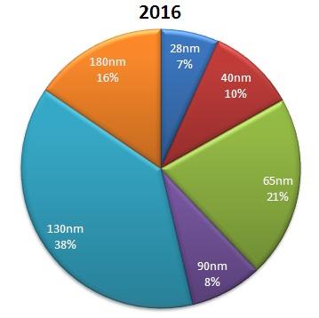
Yet again it indicates a very slow shift to more advanced nodes, and the expectationis that even in 2016 most new designs will still be done in 130nm.

This is clearly a paradigm shift in the industry, and the industry is responding accordingly.

Just prior to 2014 Semicon West, we have seen the conclusions of the SEMI’s World Fab Forecast -- Technology Node Transitions Slowing Below 32 nm. The Forecast uses a bottom-up methodology, providing high-level summaries and graphs, and in-depth analyses of capital expenditures, capacities, technology and products by fab. The chart below illustrates this new paradigm.
Picture
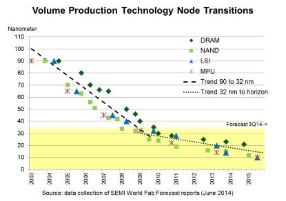
The report states: “The cost per wafer has become an increasing concern below the 32nm node.   The expected cost reduction benefit of production at smaller nodes is diminishing and is not keeping pace with the scaling benefits in many cases.  This has widespread and fundamental implications for an industry long following the cadences of Moore’s Law… These may be contributing factors as to why some volume fabs are exhibiting a lag in beginning production of a new technology node.  Now evident quantitatively for the first time, there is evidence of a clear slowdown in volume production scaling of leading technology node transitions.” (emphasis added)

This was followed by another EE Times article – Silicon Highway Narrows, Twists: “Most foundries have yet to start buying the capital equipment needed for the 14/16 nm node, which for many will be the first to support FinFETs, says Trafas of KLA-Tencor. Gear companies hope the orders start coming in the fall…Indeed, he says, one of the big questions many capital equipment execs will bring to this year's Semicon West event on July 7 is, "When will the 16/14 nm investments begin?"

In the same vein, Ed Sperling continued in Established Nodes Getting New Attention: "Work is under way to improve energy efficiency and boost performance without relying on multi-patterning or finFETs. As the price of shrinking features increases below 28nm, there has been a corresponding push to create new designs at established nodes using everything from near-threshold computing to back biasing and mostly accurate analog sensors."

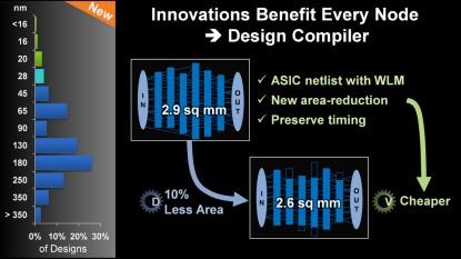
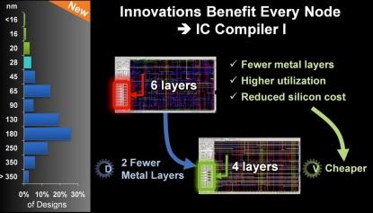
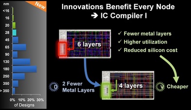
And a week later Samuel Wang, an analyst with Gartner, in Who’s Winning The FinFET Foundry Race? wrote: “Short-term, during the first two years of finFET production, there is no need for more than 50,000 wafers a month capacity from all foundries to satisfy the market demand for finFETs, …In the long run and before 2018, there is no need to have more than 250K wafers a month capacity to support the market demand for finFETs."    The EDA industry also is recognizing this paradigm shift. Dr. Aart de Geus in his keynote to the 2014 Synopsys User Group titled Designing Change Into Semiconductor Techonomics, recognized this shift with a series of slides articulating how EDA tools that were developed to support the new technology nodes could also benefit design efforts of old nodes:  
Picture
Picture
The IP industry is recognizing this paradigm shift as well, visible in IP Reaches Back To Established Nodes: "As SoC developers shift backward to established nodes, steps can be taken to improve the IP’s functionality. Driven by the IoT and wearable market opportunity, SoC developers are shifting backward to established nodes, and what is learned at the leading-edge nodes is being leveraged in reverse as IP is ported backward to improve functionality."

There also a clear effort to add value and innovation to older nodes by incorporating technology such as SOI and low Vt, known as sub-threshold designs. Most notable was the recent Samsung announcement of licensing FD-SOI from ST Micro for the established node of 28 nm. Some quotes from the articles above illustrate this trend:

* Krishna Balachandran, product marketing director for low power at Cadence. “Threshold voltage manipulation like forward biasing has been selectively used to speed up critical portions of the IP at the expense of increased leakage that is restricted to those sections of the IP without significant overall impact.”

* ARM Fellow Rob Aitken said energy savings are significant using the same exact processors differently. Moreover, it’s most effective at established process geometries where there are no finFETs. But it isn’t a simple process. (For a deeper understanding of this subject, click here). “We can get 4X to 6X improvements in energy,” said Aitken. “That doesn’t come for free, because we have to make some design changes to allow the design to operate down at this low energy point. But if we do this wrong, the overhead we have to add to get these savings is more than you get in terms of a benefit.”

* Mary Ann White, director of product marketing for the galaxy design platform at Synopsys: "Body biasing is another technique that is being recycled. It entered the picture at 90nm, when design teams found they could reduce leakage by as much as 30%. Even at 45/40nm, savings were in the 20% to 25% range. But at 28nm, the benefit for bulk CMOS dropped to as low as 2%,...When you use biasing, you are using extra tracks and extra resources, which may include one or two extra rails,” said White. “But the benefit was falling off at 28nm using planar CMOS. Interest is picking up again with FD-SOI. What’s interesting about this is we used to insert biasing at the back end, where you require a bulk n-well or p-well pin. But recently we’ve had a request to add that capability into UPF. We rolled that out with skepticism on our part, but we’ve been getting a lot of interest. If you’re adding 5% area for better power, it’s worth it.” (See related discussion.)

This paradigm shift could be a real blessing to the industry. The escalating costs drove out VCs from investing in semiconductor start-ups, drastically narrowed the number of vendors and the number of advanced new designs. It left little room for innovation or anything other than rushing to the next technology node. Now it seems that a whole new industry dynamic is taking place, innovation is being embraced, new markets are being explored, and hopefully we will see the return of VCs with the increase of semiconductor vendors and technologies.

This is also the time to pay increased attention to semiconductor technologies that could offer better intrinsic devices without traditional dimensional scaling. Most notable among those would be, SOI, Monolithic 3D, and Sub-threshold design. The 2014 S3S Conference scheduled for October 6-9, 2014, at the Westin San Francisco Airport would be a great opportunity to learn more about those technologies as it provides the latest research results along with workshops, tutorials and range of invited papers. The conference advance program is now available at < http://s3sconference.org/program/ >. It looks now to be the one conference that active members of the semiconductor industry should not miss. 

submit to reddit
0 Comments

FPGA as ASIC Alternative: Past and Future

4/28/2014

1 Comment

 
Picture
We have a guest contribution from Zvi Or-Bach, the President and CEO of MonolithIC 3D Inc. Mr. Or-Bach discusses about the FPGA as ASIC Alternative. 

In our recent blog 28nm – The Last Node of Moore's Law we outlined the recent dramatic change that has happened after many years of cost reduction associated with dimensional scaling. It is clear now that 28 nm will provide the lowest cost per gate for years to come. In this blog we will assess the potential implications for the ASIC and the FPGA markets. Over the last two decades we have seen escalating mask set costs associated with dimensional scaling and accordingly escalating NRE costs. At the recent 2014 SEMI Industry Strategy Symposium (ISS) Ivo Bolsens, Xilinx CTO, presented the following chart of ASIC design cost escalation: 
Picture
Figure 1
The dramatic increases of ASIC design cost have had a real effect on the ASIC market, reducing the number of new designs and dramatically reducing the number of vendors serving the ASIC market.

One would expect that such a trend would have a very positive effect on the FPGA market, as there is no mask-set cost associated with an FPGA design and, accordingly, far lower NRE costs per design. The following fictitious chart presented in the EE Times article: What’s the number of ASIC versus FPGA design starts?, illustrates these expectations.

Picture
Figure 2
Surprisingly, this did not really happen. The following chart presents the overall FPGA market during the last decade according to the financial results of Xilinx, Altera and Actel.
Picture
Figure 3
The FPGA market growth could be compared to the overall semiconductor market growth as presented in the chart below (the market in 2013 was $305B). Clearly the FPGA market growth during the last decade is similar to the overall semiconductor market growth, and there is no indication of any benefits from the escalating ASIC mask-set cost and its associated NRE.
Picture
Figure 4
The FPGA technology started in the mid-1980s as an alternative to the popular ASIC technology then – the Gate Array. The acronym FPGA stands for Field Programmable Gate Array. During the 1990s the Gate Array technology lost its appeal and the ~$20B Gate Array market shrunk dramatically and effectively ceased to exist. Analyst expected that this will have a dramatic positive impact on the FPGA market, which did grow some but far from the expectations. The trend of escalating NRE driven by dimensional scaling and escalating lithography costs kept on going in the 2000s and drove down the number of ASIC designs. And, again, analysts expected a huge surge in the FPGA market. Clearly, this did not happen. 

In the following we will present our theory why it did not happen and some potential implications for the future.

We believe that the stagnation of FPGA growth is mostly due to the inefficiency of the FPGA technology. Most FPGAs use SRAM as the programming or ‘switch’ technology. Interconnects are the dominating resource in modern designs. Within an SRAM based FPGA the programming of interconnects is implemented by an SRAM cell control of a pass transistor, driver, or bidirectional driver. The following chart illustrates the diffusion area associated for such Programmable Interconnect Cell (PIC) assessed in 45nm technology and compared to the size of mask-defined equivalent – the via. The results indicate that the cell area overhead for the SRAM PIC is over 30X when compared to a via, which does not include the additional circuit overhead area needed to program and control the SRAM PIC.
Picture
Figure 5
This number had been reported in the industry for many years. A 2007 research paper by Ian Kuon and Prof Jonathan Rose (IEEE Transaction on Computer-Aided Design of IC and System) says this clearly: “In this paper, we have presented empirical measurements quantifying the gap between FPGAs and ASICs for core logic. We found that for circuits implemented purely using the LUT based logic elements, an FPGA is approximately 35 times larger and between 3.4 to 4.6 times slower on average than a standard-cell implementation.”

This high programmability overhead suggests that many of the current ASIC designs cannot be replaced by an FPGA design. Consequently, when advanced technology NRE is too high, the alternative is to use older node ASIC technologies. Since the number one driver for cost of mask-sets and NRE is the associated capital, the cost of older technologies goes down dramatically over time. The 30X area penalty means that one could use a node that is five generations older and have a competitive solution when compared to current node FPGA. Taking into account the 60% gross margin of the FPGA companies and the overhead of using a fixed-sized device of an FPGA family rather than a custom tailored Standard Cell device, these could compensate for an additional two nodes. Looking again at the design costs as illustrated in the Xilinx chart above, we can see that at 180 nm the design costs are pretty low and the mask set costs are too small even to register on the chart.
What has really happened is that many designs chose to use older node standard cells instead of an FPGA. In his last keynote presentation at the Synopsys user group (SNUG 2014) Art De Geus, Synopsys CEO, presented multiple slides to illustrate the value of Synopsys newer tools to improve older node design effectiveness. The following chart is one of them and it also includes in its left side the current distribution of design starts. One can easily see that the most popular current design node is at 180nm. Clearly even such old node provides a better product than the state of the art FPGA.  
Picture
Figure 6
Now we understand why the escalating mask set and NRE costs have not resulted in a surge of FPGA designs but rather pushed designers to user older technology nodes that had depreciated enough to make their NRE cost less of an issue. The following chart of Design Starts per Node by IBS was recently presented in a Synopsys article "The new landscape of advanced design". It shows the design starts trend over time and, not surprisingly, indicates that designers migrate to more advanced nodes over a longer time and that the up and coming node these days is just 65 nm.
Picture
Figure 7 - Design Starts per Year (Source: IBS Dec 2012)
Recently EE Times published our blog, 28nm – The Last Node of Moore's Law. In it we presented that the 28nm node will be the end of cost reduction for dimensional scaling. Most analysts accept by now that 28 nm is going to be the lowest cost per gate for many years to come. 

There are potentially many implications of this change in Moore’s Law. One of those implications could affect the future of FPGAs.
Traditionally FPGAs have been, and still are, a technology driver of new logic technology nodes. This early adoption gave the FPGA customer a constantly better programmable platform for their designs. Now that dimensional scaling does not provide better cost, it will result in a build-up of pressure for FPGA customers to use a depreciated technology node as an alternative. Over time designers would see the NRE of 65nm going down to about what the 180nm NRE is today. Comparing a 65nm Standard Cell design to an FPGA of 28nm suggests that far more designs could be better off with Standard Cell. As 20 nm and 14 nm FPGAs would not provide a better cost than the 28 nm one, it means that the FPGA market could see a growing challenge in the coming years. 
 
Designers chose older nodes not just for its lower mask-set and NRE costs but also for availability of broader embedded options such as flash memories and analog cells. But those are becoming available on newer nodes over time as well. The 65 nm node is now ramping up and would become the preferred choice for new designs in a few years, as its mask-set cost and NRE keep going down thanks to deprecation and broader availability. As volume production of older designs winds down, vendors are reducing their costs to bring new designs in, and will soon make the 65 nm as easy to access as 180 nm is now. FPGA vendors will release newer products on 20nm and 14nm but those would not offer lower production costs than the 28 nm FPGA products and will be less and less competitive versus a ‘not too old’ technology node such as 65 nm. It only seems logical that these new semiconductor industry dynamics will have a negative effect on the FPGA market and a positive effect on ASIC and Structured ASIC technologies. 

Thus it behooves us to consider what can the FPGA vendors do to keep their business growth.
Interestingly, the same trend that now works against FPGA technologies could be used to improve their competitiveness. In the early days two major FPGA technologies were competing in the market. The SRAM technology and the anti-fuse technology. The SRAM technology had higher switch overhead, but ended up winning because it benefitted from two major advantages. First, it did not need any major process changes and could be adapted to newer nodes as soon as those could be fabricated. Second was their ability to reprogram the device over and over again. Now that new process nodes do not provide lower costs, FPGA vendors could look to other than SRAM technology as a new path to improve their programmable platforms. As for anti-fuse, the significant effort in recent years to develop RRAM technology opens the possibility of adopting antifuse technology that could offer re-programmability. Even more important is the fact that re-programmability these days is far less important as all FPGA designs utilize simulation technology and other EDA tools, as the trial and error methodology no longer can be effectively used for modern designs. 

A special type of antifuse programmable technology could be most effective – Antifuse-based 3D High Density FPGA. This type of programmable fabric leverages anti-fuse metal to metal technology, which use 3D transistors for programming the anti-fuses. The 3D transistors could handle the higher voltage required for the programming and provide the interconnect programming with minimal device density impact. The 3D anti-fuse programmable fabric density is very similar to a via programmable fabric. Via programmable fabrics has been used with structured ASICs such as those offered by eASIC and Triad Semiconductors (ViASIC). They provide a programmable fabric with about a 2X area penalty vs. mask-defined standard cell technologies. These antifuses could be made as one time or reprogrammable devices and be fully replaced by mask-defined vias for even lower cost volume production, as illustrated by the following chart
Picture
Figure 8
Going forward, the semiconductor industry needs to go through fundamental change. No longer is it sufficient to scale using the next node of dimensional scaling to provide better overall device value. From the 28 nm node going forward, the industry needs to open up for a broad range of innovation so to continue offering better products. We can only hope that this will drive the industry back to fast growth and support the future market of Internet-of-Things and Internet-of-Everything.
submit to reddit
1 Comment

Are We Using Moore's Name in Vain?

11/7/2013

0 Comments

 
Picture
We have a guest contribution from Zvi Or-Bach, the President and CEO of MonolithIC 3D Inc. Zvi's blog post is about Moore's Law and the impact of it on the industry today.

The assertion that Moore made in April 1965 Electronics paper was:"Thus there is a minimum cost at any given time in the evolution of the technology. At present, it is reached when 50 components are used per circuit. But the minimum is rising rapidly while the entire cost curve is falling (see graph below)." 
Picture
"The complexity for minimum component costs has increased at a rate of roughly a factor of two per year (see graph on next page). Certainly over the short term this rate can be expected to continue, if not to increase. Over the longer term, the rate of increase is a bit more uncertain, although there is no reason to believe it will not remain nearly constant for at least 10 years."
Picture
Clearly Moore's law is about cost, and Gordon Moore’s observation was that the optimum number of components (nowadays - transistors) to achieve minimum cost will double every year.
The reduction of cost per component for many years was directly related to the reduction in feature size - dimensional scaling. But many other technology improvements made important contributions as well, such as increasing the wafer size from 2" all the way to 12".
But many observers these days suggest that 28nm will be the optimal feature size with respect to cost for many years to come. Below are some charts suggesting so:
Picture
And more analytical work by IBS’ Dr. Handel Jones
Picture
Graphically presented in the following chart
Picture
Or as nicely drawn by Globalfoundries
Picture
Recently EE Times reported that EUV Still Promising on IMEC's Road Map. IMEC provided a road map to transistor scaling all the way to 5nm, as illustrated in the following chart:
Picture
Yes, we probably can keep on scaling but, clearly, at escalating complexity and with completely new materials below 7nm. As dimensional scaling requires more advanced lithography it is clear that costs will keep moving up, and the additional complexity of transistor structures and all other complexities associated with these extreme efforts will most likely drive the costs even higher.
Looking at the other roadmap chart provided by IMEC and focusing on the SRAM bit cell in the first row, the situation seems far worse:
Picture
Since at 28 nm SRAM bit cell is already 0.081μm2, this chart indicates that future transistor scaling is barely applicable to the SRAM bit cell, which effectively is not scaling any more.
Unfortunately, most SoC die area is already dominated by SRAM and predicted to be so even more in the future, as illustrated by the following chart:
Picture
Source:. Y. Zorian, Embedded memory test and repair: infrastructure IP for SOC yield, in Proceedings the International Test Conference (ITC), 2002, pp. 340–349
Dimensional scaling was not an integral part of Moore's assertion in 1965 – cost was. But dimensional scaling became the “law of the land” and, just like other laws, the industry seems fully committed to follow it even when it does not make sense anymore. The following chart captures Samsung’s view of the future of dimensional scaling for NV memory, and it seems relevant to the future of logic scaling just as well.
Picture
submit to reddit
0 Comments

EUV vs. TSV: Which one will become production ready first?

7/31/2013

1 Comment

 
Picture
We have a guest contribution today from Israel Beinglass, the CTO of MonolithIC 3D Inc. Israel debates on the answer to an important question that is on everybody's mind these days.

Like every Semicon West show in the past, where many experts are brought together for showing the latest and greatest semiconductor manufacturing equipment and bringing numerous seminar/panel discussions, this Semicon West of 2013 was no different. Two major issues were discussed, which on the face of it look unrelated, that caught my attention:

Progress in

  1. 3D - TSV technology, and
  2. EUV
Obviously these two issues are very different, but they are quite similar in respect to the following:

1. As the advanced node progresses to smaller and smaller feature size we are getting closer to the "end of the road map" or the "end of Moore's law".

Going to EUV does alleviate some of the problems related to the current solution of double patterning (or quadruple in the future assuming, EUV doesn't come to fruition soon enough).

As well, utilizing 3D devices with TSV has, in the grand scheme, a similar outcome; namely, advancing the integration via 3D structures rather than continued scaling. Though in the future, 3D devices and advanced nodes could go hand in hand.

2. The big miss of the road map. When one looks at some old road maps from a few years ago, one can ask how did we, the industry, miss by so much?

This actually reminds me of another miss from a few years ago-the low k inter-metal dielectric. Fig. 1 shows the low k dielectric roadmap trend of various ITRS published roadmaps and the prediction in 1999 that by 2004 we would be using k<2 !! Obviously we know what happened and even today 14 years later it is hard to breakthrough a k value of 2.5. 
Picture
Figure1: low k Dielectric Road Map
Figures 2 and 3 show the roadmap for EUV and TSV, respectively. Both are of 2009 vintage. In each case the prediction of the road map vs. actual is startling.
Picture
Figure 2: EUV road map
Picture
Figure 3: TSV road Map
It is not the purpose of this blog to go over the reasons why the roadmaps of EUV and TSV missed the time table by miles, nor to blame anybody for it. There are many articles and discussions published on the subjects. Rather, I will touch on some of the highlights as well as try to make some conclusions regarding the pathway of the industry regarding these two important technologies.

EUV: The EUV technology has so far gone through monumental achievements vis-à-vis the incredible tasks of developing the next generation stepper technology. The amount of engineering and resources poured into it is unprecedented in the short history of the semiconductor industry and maybe so for other industries.

It looks like as I write this blog that the only barrier for the technology from becoming a HVM tool is EUV source power that can provide a high enough throughput. Many experts doubt that it could ever be achieved; however, there are many other experts saying that it is within a reach.

TSV: In this case I could see two totally unrelated issues:

1. Technology driven obstacles

2. Logistics and supply chain issues.

In the case of the TSV it is one of the few cases where the "power point" presentation(s) of the TSV idea are so convincing that it is actually hard to oppose it. However, when it comes to the fine details of the technology development, there are many issues that still need to be addressed and resolved. I believe that it is just a matter of time before the technical obstacles will be resolved and a unified standardized solution emerges. However, on the other hand, I see a real problem from the point of view of logistics, cost and supply chain of the technology, and I have some doubts if it can ever be resolved. For further discussion on this issue, please refer to: 3D IC Supply Chain: Still Under Construction, and to a detailed comment in EE Time published blog and comments re. Semicon West 3D - IC TSV, provided here below.

In summary, I believe that the industry will come with a solution for EUV before TSV becomes a production technology.

Yet there is another alternative to TSV and to EUV - it is the Monolithic 3D methods. Moreover, it is very likely that monolithic 3D will reach volume production before EUV and TSV. As we already see the  NAND Flash vendors ramping up for production of 3D NAND.

The detailed comment fromm EE Times re. Semicon West 3D - IC  TSV:

PictureUSER RANK CEO
Re: Semicon Showed Support for 3D ICs  
chipmonk0   7/18/2013 1:46:13 PM

" same old same old ... " !! With such pollyannaish coverage, I am afraid that TSVs will remain the next hot interconnect tech even 5 years from now !

To provide a counter-point to all this happy talk, SemiCon had invited me to lead a 1 hr discussion at the Show on "Roadmap for TSVs and Alternatives from a Technology perspective ". Since Herb was not there, here are the key points :

1. unlike previous Advanced Packaging technologies like Flip Chip which we developed at IDMs like Motorola & Intel with both deep / broad expertise and product commitments, the development of TSVs has been going on mostly at overseas Govt. funded Laboratories in fits and starts and has then jumped to Foundries / OSATs. Xilinx' use of 2.5-d to integrate poorly yielding FPGAs has led to much irrational exuberance and then disappointment.

2. In the Winter of 2010 - 11 Samsung reported the first Wide I/O DRAM stack using TSVs. Great bandwidth even at 200 MHz & terrific power eff. But what the blogosphere neglected to report was that the yields were down in the mud and since then not much has been heard about Wide I/O from Samsung. Instead they keep bringing out conventional LP DDR at ever higher Clock Rates. JEDEC has actually postponed Wide I/O to 2015. 
3.  The development of TSV technology has been going on in Fabs who do not have to be sensitive to stress issues common in "thick film" type laminates / composites as is the case for filled vias. It is only now that they are waking up to it. Stress effects depend on the sq. of via dia., hence the new interest in shrinking them below 5 um. But integration & reliability problems ( at high Aspect Ratios both get worse ) have not been thought through. Moreover, Bonding stacked chips using the current method ( a sort of pidgin version of the technology I had invented nearly 20 years ago at Motorola for GaAs Power Amps that went into Cell Phones ) also introduces residual stress, affects electron mobility and shifts timing. 

4. While these slow-poke Govt. funded Euro Labs rediscover stress effects on device perf. and the perils of Cu metallurgy applied indiscriminately, there is at least one small Company outside Chicago that has already shifted to the non - obvious ( at least to these TSV-niks ) yet theoretically sound choice of using Tungsten ( a brittle and poor electrical conductor which can be compensated by Design but unlike Cu a close CTE match with Si ).

5. But thats not all Folks - this tiny Co. with just 3 PhDs and Physicists has also solved the biggest TSV integration problem thats keeping all these Labs and various Tool Vendors new to the game ( in Herb's Osterreich they love to build big complex "Maschine" - Physics be damned ) -- intent on optimizing their individual process steps ( e,g. back up wafer bond / debond ) at the risk of compromising the whole process -- awake at night.

6. We did cover more, e,g. as to how to get the electrical benefits of TSVs w/o actually having to drill holes in live Silicon, circuitry and packages that make it possible. We already have some of these Alternatives ( using the concept of Active Interconnects ) under development - especially for the very large Server & SmartPhone markets - and have started publishing.

7. TSV development is orders of magnitude more complex than Flip Chip and would benefit from the same type of brutal, theory-driven Program Management practiced at the world's largest semiconductor Co., but since they have money in the Bank to stay on Moore's Law and thus continue single chip solutions they don't need TSVs that badly. So unless there is a radical shake - up in the TSV programs "outside", incl. at the Foundries, the present slow pace of TSV development will persist.

Morale : give TSVs a fair chance, they need a respite from these overly enthusiastic bloggers, embarassingly out of their depth, and at Conferences lets not blather about Supply Chain Issues, the technical probems are not all solved yet
submit to reddit
1 Comment

IEDM: Moore’s Law seen hitting big bump at 14 nm

12/13/2012

0 Comments


Imec's Luc van den Hove vs. Intel's Mark Bohr

Picture
We have a guest contribution from Zvi Or-Bach, the President and CEO of MonolithIC 3D Inc. Zvi discusses EE Time's article about: "Moore's Law seen hitting big bump at 14 nm".

The EE Times article covering Imec's Luc van den Hove keynote talk at IEDM 2012 reports: "Chips made at the 14-nm process node may deliver as little as half the typical 30 percent performance increase - and still carry a hefty cost premium - due to the lack of next-generation lithography". Van den Hove provided the following slide photo as an illustration:
Picture
Yet, in an article about Intel's 22nm IEDM presentation, EE Times is quoting Mark Bohr of Intel: "Projections from an IMEC keynote that 14-nm wafers will be 90 percent more expensive than 28-nm parts due to the lack of EUV lithography are inaccurate, Bohr asserted. The cost increase for 14-nm wafers at Intel "is nowhere near that," he said. "Cost per wafer has always gone up marginally each generation, somewhat more so in recent generations, but that’s more than offset by increases in transistor density so that the cost per transistor continues to go down at 14 nm," Bohr said.


So who is right between those two giants?

Could it be that both of them are?

In a recent blog titled "Is the Cost Reduction Associated with Scaling Over?" we presented charts clearly supporting Luc van den Hove, IMEC's CEO, position. The following slide from an IBM presentation includes an NVidia chart (which we also discussed in another blog, Is NVIDIA in a Panic? If so, what about AMD? Other fabless companies? ).
Picture
Accordingly, it would seem that TSMC wafer costs are in line with Luc and so is the case with IBM.

GlobalFoundries, in its recent 14nm announcement, disclosed that the back-end will be unchanged from 20nm. This suggests a similar die size and respective increase in per-transistor cost. Further, ST Micro in the Fully Depleted Transistors Technology Symposium yesterday (Dec. 11) also acknowledged that their 14nm node will have a 20nm node metal pitch and, just like GlobalFoundries, a similar die size and increase in per-transistor cost.
In other words, it seems that the Luc van den Hove keynote is in-line with the cost road map of the non-Intel foundries!

Intel might indeed be different, yet something did cause Intel to take what seems like an extreme measure, when it put $4.1B in ASML just recently.

If, however, Mark Bohr has not been misled by the Intel accounting department, and the Intel process is still providing a nice cost reduction at every node of scaling, then clearly Intel has a true competitive edge relative to all other foundries. I have no doubts that Intel has filed enough patents to protect its unique process advantage, but then I wonder why did Mark say: "However...we don't intend to be in the general-purpose foundry busines ... [and] I don't think the [foundry] volumes ever will be huge [for Intel]."
If Mark Bohr is right, with such a competitive edge Intel should aggressively expand its foundry business, which would achieve both a great profit margin and rapid business growth. Now that Intel is looking for a new CEO its Board should consider it as a major criterion for who should lead Intel into the future.

P.S.

Clearly, dimensional scaling (and its cost reducing benefits) is not what it used to be, and the market appetite for cheaper-faster-better consumer-oriented products grows stronger. Both Intel and non-Intel fabs should start development of monolithic 3D technology.  ;-)
submit to reddit
0 Comments

Qualcomm overtakes Intel in market capitalization

11/13/2012

0 Comments

 
"Only the paranoid survive"
Picture
We have a guest contribution from Zvi Or-Bach, the President and CEO of MonolithIC 3D Inc. Zvi discusses about Qualcomm overtaking Intel in market capitalization.

On Nov 9, 2012 we learned that Qualcomm overtook Intel in market capitalization. Quite shocking news if one considers that Intel’s revenue is almost three times that of Qualcomm and its net margin is more than twice that of Qualcomm. Clearly investors evaluate Qualcomm using a different scale than what they use for Intel, as is evidenced by Qualcomm’s P/E of 20.12 vs. Intel's mere 9.07. EE Times explained it in an article that day stating: "In the eyes of investors who have driven up its market capitalization, the fact that Qualcomm is a fabless company relieves it of the burden of having to invest billions of dollars each year in process development and wafer fabs." However, given that TSMC, a pure foundry, has a P/E of 15.67, it behooves us to look for another explanation. It’s also worth noting that TSMC had a revenue growth of 2% in the last year, far less than Intel's 25.6%, and its net income actually went down vs. a net income growth by Intel of 213%!

My explanation is that it is all about IP strength. I will expand on it in the rest of this blog but as prime evidence I offer SanDisk, who sports a P/E of 20.78  yet has continued to invest heavily, together with its partner Toshiba, in fab capacity upgrades.

Let’s first look at the previous two decades as Intel grew consistently year after year while riding the PC business growth. During those years the team Intel + Microsoft was the exclusive vendor in the PC 'game'. All others had to compete neck to neck in this fast growing commodity market.  And as we all know, broad competition erodes margins and allows only the lowest cost producer to achieve some profits. In the case of PC this erosion actually pushed out the market creator - IBM - which eventually exited the market and sold its business to Lenovo. The only real winners back then were Microsoft and Intel, who had pivotal differentiating IP. Yes, Intel had a licensor - AMD - but as a licensor, AMD had to pay heavy royalties that impacted its profits, and helped those of Intel.

Both Intel and Microsoft were able to leverage there unique IP into years of growth and became the largest companies in their field.

But being the largest today does not guarantee the tomorrow. Or, as Andy Grove famously said, "only the paranoid survive".

The technology world is about change. While many of the changes are incremental, at times the paradigm changes too. The change that took away Intel’s and Microsoft’s unchallenged market and IP position was the shift to "smart mobile," or mobile internet, as is illustrated in the following chart.
Picture
The technology world is about change. While many of the changes are incremental, at times the paradigm changes as well
And with these changes new technology leaders have been emerging: companies such as  Apple, Qualcomm, and Google.

To make matters even worse, a small company - ARM - was able to create a disruptive change in the computing engine with its preferred computing architecture, first for 'smart mobile,' then for tablets, and now it seems to penetrate the PC and the server markets.

In my view, as soon as the investment community realized that Intel’s exclusive market and IP position is not relevant to the new market of Mobile Internet, it started to tune down Intel’s P/E. This trend even got stronger as investors became concerned regarding Intel’s position in the PC and server market.

It should be noted that in this context IP is not counted by the number of patents or the amount of trade secrets but rather by the ability to exclude competitors from major markets or extract royalties from those competitors, which may make you a winner even when you loose business. This is a status that Qualcomm and other companies such as SanDisk enjoy.


Economists estimate that two-thirds of the value of large businesses in the U.S. can be traced to intangible assets.[18] "IP-intensive industries" are estimated to generate 72 percent more value added (price minus material cost) per employee than "non-IP-intensive industries".[19][dubious – discuss] , as is illustrated by the following chart
Picture
So, is the game over for Intel??? Is the Market irrational, or is the Market perceptive?

Some pundits clearly think so, but given its leadership semiconductor technology, strong leading edge manufacturing infrastructure, and balance sheet, it is way too soon to call game over for Intel. But it would seem that Intel needs to introduce some real change in order to correct its course. Perhaps Intel should look back at what Andy Grove’s said and ask itself: does it really act like a paranoid company, or perhaps it is just the inverse.

We at MonolithIC 3D believe that the whole semiconductor industry is about to go through a major disruptive change. After 50 years of successful growth and progress by dimensional scaling, the time has come for a direction change, and the time is now for starting to embrace scaling-up, going for monolithic 3D. The current leaders in dimensional scaling, the NAND Flash vendors, seem to be leading the way. They are pushing ahead with monolithic 3D-NAND. This disruptive change will bring vast new opportunities, and those who will be early to embrace the change may be able to reap the IP reward.
submit to reddit
0 Comments

Happy Thanksgiving

11/24/2011

0 Comments

 
Picture

We have a guest contribution today from Iulia Morariu, who works in our Romanian team. Iulia is an energetic and creative person who has been doing great things for our marketing division. She will give a thanksgiving greeting.


Read More
0 Comments

How Korea Became the Hub of the Memory Industry

11/20/2011

7 Comments

 
As you'd know, Korean companies such as Samsung and Hynix contribute 50-60% of the world's memory revenues. In today's blog post, we’ll look at reasons and strategies behind this dominance...

Read More
7 Comments

    Search Blog


    Meet the Bloggers


    Follow us


    To get email updates subscribe here:


    Recommended Links

    3D IC Community
    3D IC LinkedIn Discussion Group

    Recommended Blogs

    • 3D InCites by Francoise von Trapp
    • EDA360 Insider by Steve Leibson
    • Insights From the Leading Edge by Phil Garrou
    • SemiWiki by Daniel Nenni, Paul Mc Lellan, et al.

    Archives

    March 2022
    December 2021
    August 2021
    August 2018
    July 2018
    May 2018
    October 2017
    September 2017
    December 2016
    September 2016
    August 2016
    November 2015
    October 2015
    September 2015
    July 2015
    June 2015
    May 2015
    April 2015
    March 2015
    February 2015
    October 2014
    September 2014
    August 2014
    July 2014
    June 2014
    May 2014
    April 2014
    March 2014
    February 2014
    January 2014
    December 2013
    November 2013
    October 2013
    September 2013
    August 2013
    July 2013
    March 2013
    February 2013
    January 2013
    December 2012
    November 2012
    October 2012
    August 2012
    June 2012
    May 2012
    April 2012
    March 2012
    February 2012
    January 2012
    December 2011
    November 2011
    October 2011
    September 2011
    August 2011
    July 2011
    June 2011
    May 2011
    April 2011
    March 2011

    Categories

    All
    3d Design And Cad
    3dic
    3d Ic
    3d Nand
    3d Stacking
    3d Technology
    Brian Cronquist
    Dean Stevens
    Deepak Sekar
    Dram
    Education
    Heat Removal And Power Delivery
    Industry News
    Israel Beinglass
    Iulia Morariu
    Iulia Tomut
    Monolithic3d
    Monolithic 3d
    MonolithIC 3D Inc.
    Monolithic 3d Inc.
    Monolithic 3d Technology
    Moore Law
    Outsourcing
    Paul Lim
    Repair
    Sandisk
    Semiconductor
    Semiconductor Business
    Tsv
    Zeev Wurman
    Zvi Or Bach
    Zvi Or-Bach

    RSS Feed

© Copyright MonolithIC 3D Inc. , the Next-Generation 3D-IC Company, 2012 - All Rights Reserved, Patents Pending