Imec's Luc van den Hove vs. Intel's Mark Bohr

We have a guest contribution from Zvi Or-Bach, the President and CEO of MonolithIC 3D Inc. Zvi discusses EE Time's article about: "Moore's Law seen hitting big bump at 14 nm".
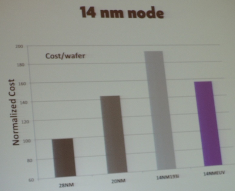
The EE Times article covering Imec's Luc van den Hove keynote talk at IEDM 2012 reports: "Chips made at the 14-nm process node may deliver as little as half the typical 30 percent performance increase - and still carry a hefty cost premium - due to the lack of next-generation lithography". Van den Hove provided the following slide photo as an illustration:
Yet, in an article about Intel's 22nm IEDM presentation, EE Times is quoting Mark Bohr of Intel: "Projections from an IMEC keynote that 14-nm wafers will be 90 percent more expensive than 28-nm parts due to the lack of EUV lithography are inaccurate, Bohr asserted. The cost increase for 14-nm wafers at Intel "is nowhere near that," he said. "Cost per wafer has always gone up marginally each generation, somewhat more so in recent generations, but that’s more than offset by increases in transistor density so that the cost per transistor continues to go down at 14 nm," Bohr said.
So who is right between those two giants?
Could it be that both of them are?
In a recent blog titled "Is the Cost Reduction Associated with Scaling Over?" we presented charts clearly supporting Luc van den Hove, IMEC's CEO, position. The following slide from an IBM presentation includes an NVidia chart (which we also discussed in another blog, Is NVIDIA in a Panic? If so, what about AMD? Other fabless companies? ).

Accordingly, it would seem that TSMC wafer costs are in line with Luc and so is the case with IBM.
GlobalFoundries, in its recent 14nm announcement, disclosed that the back-end will be unchanged from 20nm. This suggests a similar die size and respective increase in per-transistor cost. Further, ST Micro in the Fully Depleted Transistors Technology Symposium yesterday (Dec. 11) also acknowledged that their 14nm node will have a 20nm node metal pitch and, just like GlobalFoundries, a similar die size and increase in per-transistor cost.
In other words, it seems that the Luc van den Hove keynote is in-line with the cost road map of the non-Intel foundries!
Intel might indeed be different, yet something did cause Intel to take what seems like an extreme measure, when it put $4.1B in ASML just recently.
If, however, Mark Bohr has not been misled by the Intel accounting department, and the Intel process is still providing a nice cost reduction at every node of scaling, then clearly Intel has a true competitive edge relative to all other foundries. I have no doubts that Intel has filed enough patents to protect its unique process advantage, but then I wonder why did Mark say: "However...we don't intend to be in the general-purpose foundry busines ... [and] I don't think the [foundry] volumes ever will be huge [for Intel]."
If Mark Bohr is right, with such a competitive edge Intel should aggressively expand its foundry business, which would achieve both a great profit margin and rapid business growth. Now that Intel is looking for a new CEO its Board should consider it as a major criterion for who should lead Intel into the future.
P.S.
Clearly, dimensional scaling (and its cost reducing benefits) is not what it used to be, and the market appetite for cheaper-faster-better consumer-oriented products grows stronger. Both Intel and non-Intel fabs should start development of monolithic 3D technology. ;-)


 RSS Feed