Yes, unless we Augment Dimensional Scaling with monolithic 3D-IC Scaling

We have a guest contribution from Zvi Or-Bach, the President and CEO of MonolithIC 3D Inc. Zvi discusses about Cost Reduction Associated with Scaling.
The last 50 years of the semiconductor industry have been all about the manifestation of Moore's Law in dimensional scaling of Integrated Circuits (ICs). As consumers of electronic devices we all love to see with every new product cycle better products at a lower cost. But now storm clouds are forming, as was recently publicly expressed "Nvidia deeply unhappy with TSMC, claims 20nm essentially worthless".
Clearly dimensional scaling is no longer associated with lower average cost per transistor. The chart below, published by IBS about a year ago, shows the diminishing benefit of cost reduction from dimensional scaling. In fact, the chart indicates that the 20nm node might be associated with higher cost than the previous node.
Clearly dimensional scaling is no longer associated with lower average cost per transistor. The chart below, published by IBS about a year ago, shows the diminishing benefit of cost reduction from dimensional scaling. In fact, the chart indicates that the 20nm node might be associated with higher cost than the previous node.
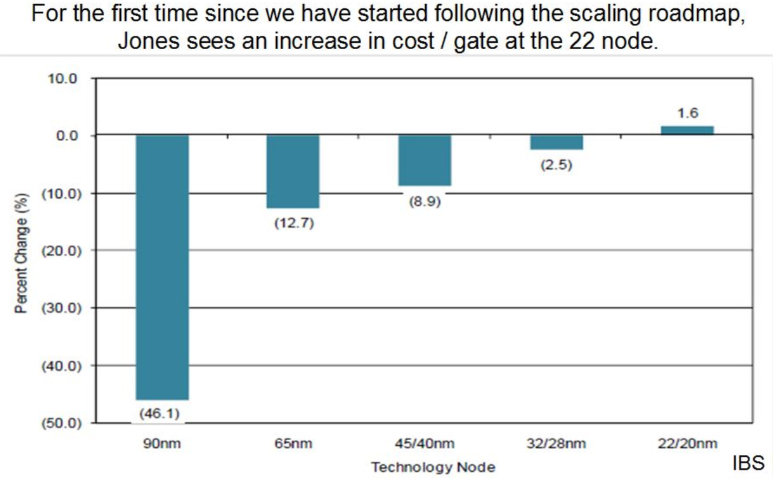
Figure 1
The following Nvidia chart provides the first order explanation. The cost reduction of dimensional scaling resulted from doubling the number of transistors per wafer. But if the wafer cost of the new technology node increases by too much then it neutralizes that cost reduction. The Nvidia chart shows the wafer cost of recent nodes over time. In the past (...80nm, 55nm, 40nm) the incremental wafer cost increases were small and rapid depreciation of those costs resulted in almost constant average wafer price. Recent nodes (28nm, 20nm, 14nm, ...), however, signal a new reality.
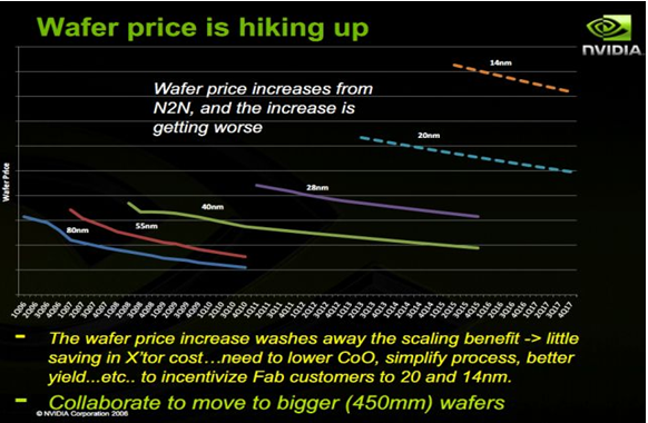
Figure 2
The following busy slide of IBM summarizes it clearly: "Net: neither per wafer nor per gate showing historical cost reduction trends"
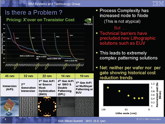
Figure 3
The number one driver to the increase of wafer cost is the increase in the equipment cost required for processing the next technology node. The following chart presents the increase in costs of capital, process R&D, and design.
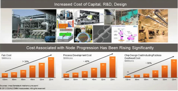
Figure 4
The sharp increase of costs associated with scaling is a new phenomenon. There were always costs to move from one node to the next, but they were about constant or incrementally small.
The following slide presents the innovations that enable dimensional scaling. Clearly, for many nodes we were able to use the same lithography tools. But once dimensional scaling reached the limit of light wavelength the lithography tool became critical and dominant. About for every node the lithography became a major challenge that required newer equipment and substantial process R&D. Moreover, in the recent lithography nodes the transistor itself required significant innovation at every node (high-k, Metal Gate, Strain, SiGe, Tri-gate,...) and it is clear that future scaled nodes will require even more of those innovations and their associated costs.
The following slide presents the innovations that enable dimensional scaling. Clearly, for many nodes we were able to use the same lithography tools. But once dimensional scaling reached the limit of light wavelength the lithography tool became critical and dominant. About for every node the lithography became a major challenge that required newer equipment and substantial process R&D. Moreover, in the recent lithography nodes the transistor itself required significant innovation at every node (high-k, Metal Gate, Strain, SiGe, Tri-gate,...) and it is clear that future scaled nodes will require even more of those innovations and their associated costs.
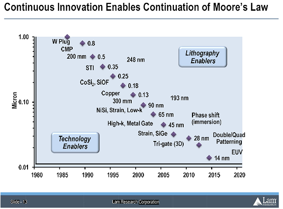
Figure 5
An important part of these costs is the escalating cost of the capital equipment for the next node fabrication lines. The following figure present the cost dynamic for the lithography equipment. Note the logarithmic scale of the cost axis.
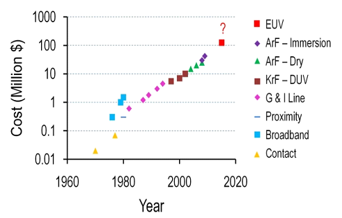
Figure 6
Lithography tools grew from less than 10% of wafer fab equipment (WFE) spending to over 25% and accordingly lithography now represents about 50 % of the wafer cost.
An interesting implication of growing domination of lithography in semiconductor processing is the fact that the ASML, which is the lead vendor of lithography tool, recently passed Applied Material’s (the leader of all other tools) market cap. Following is the chart of the stock price of ASML (in red) vs. Applied Material (AMAT).
An interesting implication of growing domination of lithography in semiconductor processing is the fact that the ASML, which is the lead vendor of lithography tool, recently passed Applied Material’s (the leader of all other tools) market cap. Following is the chart of the stock price of ASML (in red) vs. Applied Material (AMAT).
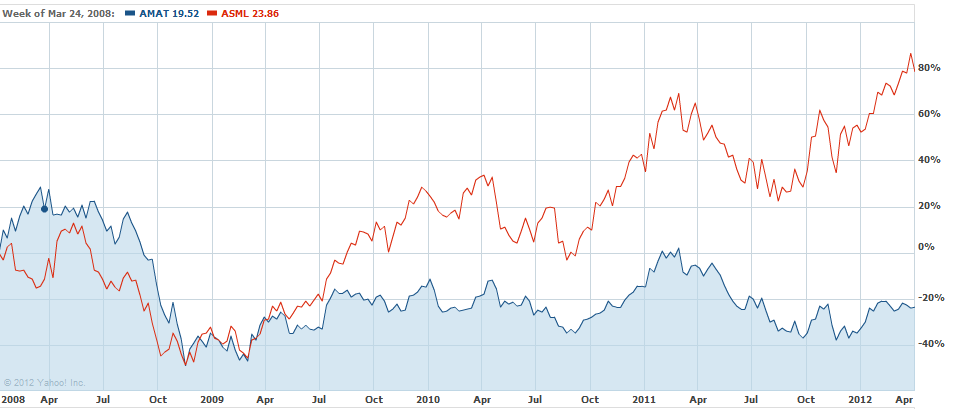
Figure 7
The clear conclusion of all of this is that future dimensional scaling is not about to change these trends. Accordingly, as stated in the IBM slide above: "Net: neither per wafer nor per gate showing historical cost reduction trends." Unless ...
Unless we change the way we do scaling (remember Einstein’s famous quote). Moore’s Law is about doubling the number of transistors in a semiconductor device. At that time dimensional scaling was one of the three trends Moore described that would enable the observed and predicted exponential increase of device integration. It would seem that it is about time to look on another one of those - increasing the die size. If we do it by using the 3rd dimension – monolithic 3D-IC – we can achieve both higher integration and cost reduction!
It is not that we should stop scaling down, it just that if we augment it with scaling up we can introduce the required changes that can achieve the continuation of the cost reduction trend. Clearly almost all of the increases of wafer costs are related to the pace of dimensional scaling. If those costs could be spread over four years instead of two then the increase in wafer cost would be only about half of what it is now.
It might not be so clear, however, why monolithic 3D should reduce wafer cost. Shouldn’t the cost of the double die size spread over two layers be at least double …?
Monolithic 3D IC would reduce wafer cost because of the following elements:
1. Reduced Die Size - It has been shown in many research studies that each folding into 3D has the potential to reduce the total required silicon area by 50% due to the reduced re-buffering and reduced sizing of the buffers.
2. Depreciation - Scaling up enables the use of the same fab and process R&D for few additional years with the associated improvement in deprecation costs and improved manufacturing efficiencies and yield.
3. Heterogeneous Integration - Scaling up would enable heterogeneous integration. This will open up the third trend of Moore- improved circuit design. As each strata of 3D IC could be processed in a different flow, cost and power could be saved by using a different process flow for logic, memory and I/O.
4. Multiple Layers Processed Together - This would be most effective for a memory type circuits. Using the right architecture, multiple transistors layers could be process simultaneously with the result of a huge reduction of cost per layer.
Let’s detail each of these.
Reduced Die Size
Dimensional scaling has always been associated with an increase of wire resistivity and capacitance. The industry had spent a huge effort to overcome these by first replacing the conducting material with copper and then changing the isolation material to low-K dielectrics. But the interconnect problem is still growing as demonstrated in the following chart.
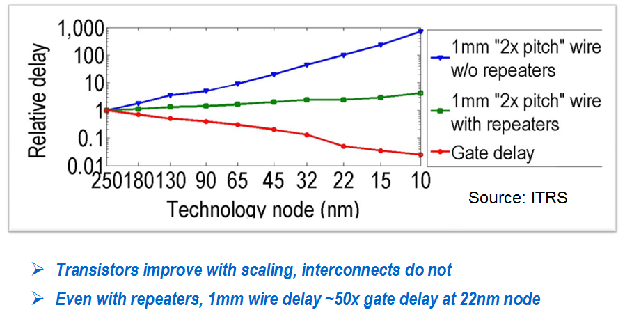
Figure 8
Every node of dimensional scaling is associated with larger cells, output drivers, and more buffers and repeaters. Monolithic 3D enables one to fold the circuit where the next strata is about 1µ above with a very rich vertical connectivity between the strata. The following IBM/MIT slide illustrates the effectiveness of such folding.
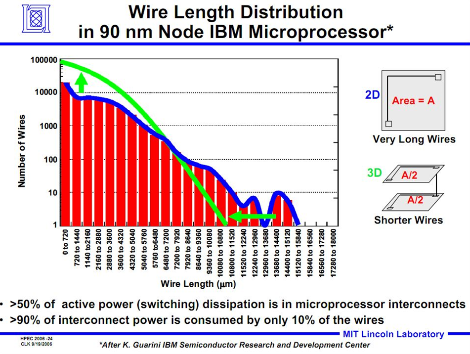
Figure 9
Further, the reduced silicon area generates an additional reduction of buffers and the average transistor size. MonolithIC 3D Inc. released an open-source top level simulator IntSim v2.0 to simulate a given design’s expected size and power based on process parameters and the number of strata (more than 300 copies have been downloaded so far).
Using the simulator we can see in the following table that a design that uses 50 mm2 with average size gate size of 6 W/L, will need an average gate size of 3 W/L and accordingly only 24 mm2 if folded into two strata (the footprint will be therefore just 12 mm2).
Using the simulator we can see in the following table that a design that uses 50 mm2 with average size gate size of 6 W/L, will need an average gate size of 3 W/L and accordingly only 24 mm2 if folded into two strata (the footprint will be therefore just 12 mm2).
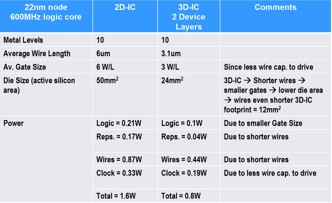
Figure 10
These results are in-line with many other monolithic 3D research results.
Depreciation
The semiconductor industry is very capital intensive and a very significant part of the wafer cost is associated with the cost of capital. Since every two years we have been scaling to a new node, then the wafer cost needs to support this rapid loss of capital value. Achieving the next level of device functionality using the same generation of tools allows for a far better utilization of the investment capital. In addition the learning curve of yield and manufacturing efficiency contributes further to the end-product cost reduction. The following chart portion demonstrates this well known trend.
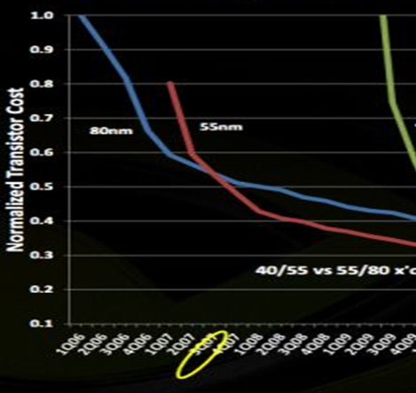
Figure 11
Heterogeneous Integration
Let’s start with quoting Mark Bohr, in charge of Intel’s process development:
"Bohr: One important perspective is that chip technology is becoming more heterogeneous. If you go back 10 or 20 years ago, it was homogenous. There was a CMOS transistor, it was the same materials for NMOS and PMOS, maybe different dopant atoms, and that basic CMOS transistor fit the needs of both memory and logic. Going forward we’ll see chips and 3D packages that combine more heterogeneous elements, different materials, and maybe transistors with very different structures whether they’re for logic or memory or analog. Combining these very different devices onto one chip or into a 3D stack—that’s what we’ll see. It will be heterogeneous integration"
The most important market for semiconductor products is smart mobility. For this market the SoC device needs to integrate many functions. In most cases the pure high-performance logic would be about 25% of the die area, 50% would be memories and the rest would be analog functions such as I/O. In 2D they all need to be processed together and bear the same manufacturing costs. In a monolithic 3D-IC stack using heterogeneous integration each stratum is processed in an optimized flow, allowing for a significant cost reduction. The following illustration suggests the use of only two strata to build a device that in 2D would have a size of 196 mm2. By having one stratum for logic and one for memory, and by using DRAM instead of SRAM, the device could be reduced to 98 mm2 with footprint of 49 mm2. The device cost would be further reduced by the memory using only 3 or 4 metal layers.
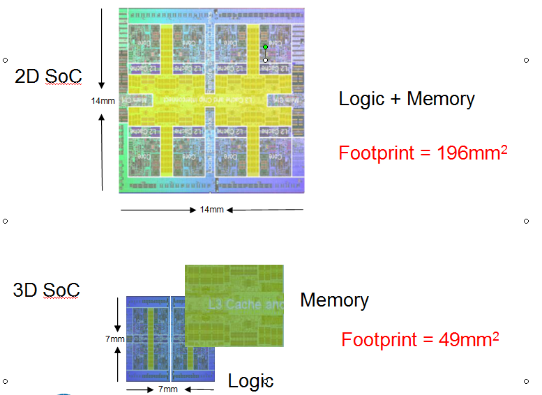
Figure 12
Multiple Layers Processed Together
Using the right architecture, multiple transistor layers could be processed together with a huge reduction in cost per layer. This could be applied to many different types of regular devices.
The following illustrate the concept with respect to a floating-body DRAM:
Using the right architecture, multiple transistor layers could be processed together with a huge reduction in cost per layer. This could be applied to many different types of regular devices.
The following illustrate the concept with respect to a floating-body DRAM:
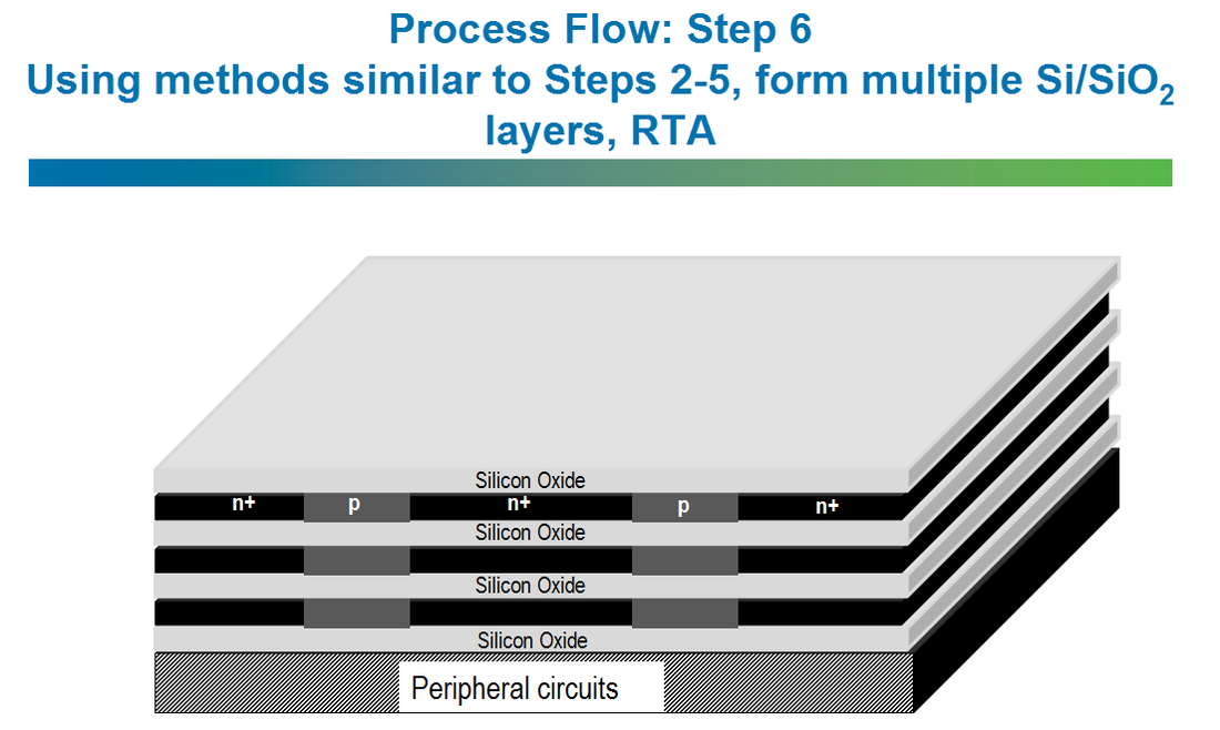
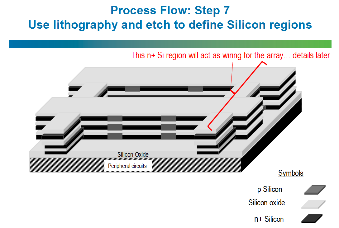
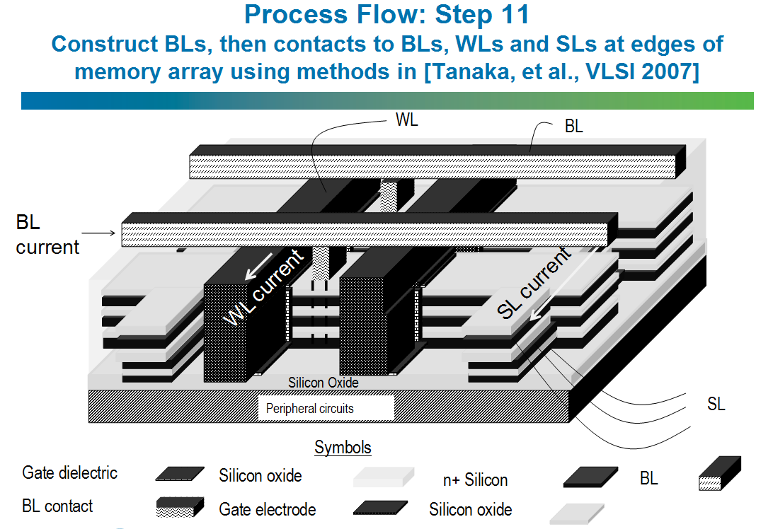
MonolithIC 3D Inc’s website presents more details for the DRAM flow, and also related flows for RRAM and NAND Flash memories.
In short, we do have a path to continue the semiconductor industry drive for better products and with lower costs, but we should continuously apply innovation to do so. Now that monolithic 3D is practical, it is time to augment dimension scaling with monolithic 3D-IC scaling.
In short, we do have a path to continue the semiconductor industry drive for better products and with lower costs, but we should continuously apply innovation to do so. Now that monolithic 3D is practical, it is time to augment dimension scaling with monolithic 3D-IC scaling.


 RSS Feed