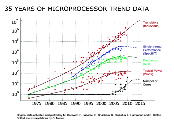
Monolithic 3D Inc., the Next Generation 3D-IC Company
  • Home
  • Technology
    • Technology
    • Papers, Presentations and Patents
    • Overview >
      • Background
      • Why Monolithic 3D?
      • Paths to Monolithic 3D
      • Applications
    • Ion-Cut: The Building Block
    • Monolithic 3D Logic >
      • RCAT
      • HKMG
      • Laser Annealing
      • RCJLT
      • 3D Embedded RAM
      • 3D Gate Array
      • FPGA
      • Ultra Large Integration - Redundancy and Repair
    • Monolithic 3D Memory >
      • 3D DRAM
      • 3D Resistive Memories
      • 3D Flash
    • Monolithic 3D Electro-Optics >
      • 3D Image Sensors
      • 3D Micro-Displays
  • 3D-IC Edge
    • 3D-IC Edge
  • News & Events
    • News & Events
    • S3S15 Game Change 2.0 Video/P
    • Webcast
    • Webinar
    • Press Releases
    • In the News
    • Upcoming Events
  • About Us
    • About Us
    • History
    • Team
    • Careers
    • Contact Us
  • Blog
  • Simulators

DARPA calls for >50x improvement in SoC using Monolithic 3D – 3DSoC

10/2/2017

0 Comments

 
Picture
We have a guest contribution from Zvi Or-Bach, the President and CEO of MonolithIC 3D Inc.
A technology that could bridge the processor memory gap, Monolithic 3D has DARPA's attention. The agency wants proposals by Nov 6. Learn more at an upcoming IEEE conference.

On Sept 13 the Defense Advanced Research Projects Agency (DARPA) launched a giant funding effort to ensure the United States will sustain the pace of electronic innovation vital to both a flourishing economy and a secure military. Under the banner of the Electronics Resurgence Initiative (ERI), some $500-$800 million will be invested in post-Moore’s law technologies.

Among those is the 3DSoC program. “The overall goal of the Three Dimensional Monolithic System-on-a-Chip (3DSoC) program" DARPA wrote in a statement, "is to develop 3D monolithic technology that will enable > 50X improvement in SOC digital performance at power. 3DSoC aims to drive research in process, design tools, and new compute architectures for future designs while utilizing U.S. fabrication capabilities.” As is illustrated in the following chart:
Picture
The foundation for the 3DSoC program were formed in prior DARPA research work performed by Stanford University in collaboration with Berkeley and CMU, Energy-Efficient Abundant-Data Computing: The N3XT 1,000×
The underlying problem enabling these orders of magnitude improvement is often called “The Memory Wall” illustrated by the following chart from Hennessy and Patterson:
Picture
The main source of the gap is the limited number of long wires connecting memory to processor. This is driven by the fact that typically the process line for memory is very different than of processor, resulting in memory chips aggregated to memory modules and being connected to the processor using printed circuit board or, at best, carrier substrate. A technology that could bridge this gap — Monolithic 3D — has the potential to provide more than 1,000x better computers.

DARPA kept the target enhancement to only 50x to allow use of chip manufactured in domestic older fab (~90nm) instead of off-shore 7nm fab lines.

Proposals are due by Nov 6, allowing everyone a unique opportunity to hear an invited talk about the program on October 16 from the 3DSoC DARPA Program Manager, Dr. Linton Salmon during this year’s IEEE S3S 2017 at the Hyatt Regency at the San Francisco Airport. The IEEE S3S conference is dedicated to monolithic 3D technologies. It provides unparalleled opportunity for quick catch up with the broad spectrum of monolithic technologies.

At the conference’s start Al Fazio, Intel Senior Fellow, will deliver a plenary talk on how 3D NAND and 3D XPoint ended being the trailblazing monolithic 3D IC technologies that have matured to volume production, taking over the fast growing memory market. The first day will conclude with two 3D IC focus sessions comprised of a mix of invited and submitted papers covering exotic technologies and the use of the emerging nano-wire transistors for 3D scaling.

The first half of the second day includes a collaborative event organized by Qualcomm and CEA Leti — the COOLCUBE/3DVLSI Open Workshop. The second half includes an open 3D tutorial providing full coverage of the various 3D integration technologies from TSV to Sequential Integrations. 

The third day is made of four sessions of invited and submitted talks on monolithic and other forms of 3D integration. These sessions include a talk by MonolithIC 3D Inc. in which we will present a monolithic 3D technology that is ready to be rapidly deployed using the current transistor process. We will also describe how such an integration technology could be used to improve performance, reduce power and cost of most computer systems, suggestive of a 1,000x total system benefit.

In addition, the IEEE S3S conference includes full coverage of SOI and low-power technologies, making it the place to be and to learn about alternative technologies to dimensional scaling. I am looking forward to seeing you at the S3S from October 16th thru 19th, 2017.
​

submit to reddit
0 Comments

DARPA calls for Monolithic 3D – 3DSoC

9/20/2017

0 Comments

 
Picture
               We have a guest contribution from Zvi Or-Bach, the President and CEO of MonolithIC 3D Inc.
​               Learn all about Monolithic 3D at IEEE S3S.


On Sept 13 DARPA come out with Electronic Resurgence Initiative (ERI) programs. Quoting: “with an eye toward the times we now live in, [Gordon Moore] laid out the technical directions to explore when the conditions under which scaling will be the primary means for advancement are no longer met. A trio of simultaneously-released ERI BAAs—this one among them—parallel the research areas detailed on page three of Moore’s paper: materials and integration, architecture, and design. These new page-three-inspired investments, along with a series of related investments from the past year, comprise the overall Electronics Resurgence Initiative.”  

Among these programs is the “Three Dimensional Monolithic System-on-a-Chip (3DSoC): Develop 3D monolithic technology that will enable > 50X improvement in SoC digital performance at power.”

In perfect timing, this year’s IEEE S3S 2017 at the Hyatt Regency at the San Francisco Airport will feature a comprehensive show case for monolithic 3D IC technologies.

At the start Al Fazio, Intel Senior Fellow, will give a plenary talk on how 3D NAND and 3D XPoint™ happened to be the trailblazing monolithic 3D IC technologies that have matured to volume production, taking over the fast growing memory market. The first day will end with two 3D IC focus sessions comprised of a mix of invited and submitted papers covering exotic technologies and the use of the emerging nano-wire transistor for 3D scaling.

The first half of the second day includes a collaborative event organized by Qualcomm and CEA Leti – the COOLCUBE/3DVLSI Open Workshop. The second half will include an open 3D tutorial providing full coverage of the various 3D integration technologies from TSV to Sequential Integrations. 

The third day of the conference will include a full day with four sessions of invited and submitted talks on monolithic and other forms of 3D integration. These sessions will include a talk by us, MonolithIC 3D Inc., in which we will present a monolithic 3D technology that is ready to be rapidly deployed using the current transistor process. In that talk we will also describe how such an integration technology could be used to improve performance, reduce power and cost of most computer systems, suggestive of a 1,000x total system benefit.

In addition, the IEEE S3S conference will have full coverage of SOI and low power technologies, making it the place to be and to learn about alternative technologies to dimensional scaling. I am looking forward to seeing you at the S3S from October 16th thru 19th, 2017.
submit to reddit
0 Comments

Happy Holidays and Happy New Year

12/24/2016

0 Comments

 
Picture
As we come to the end of 2016, MonolithIC 3D Inc. team would like to share its holiday greetings by wishing you Merry Christmas and a Happy New Year. We end this year with a grate recognition by Solid State's Magazine. Our CEO's recent blog post Moore’s Law did indeed stop at 28nm was number 1 of 2016 top stories. You can access the entire article here. 
submit to reddit
0 Comments

Moore's Law did indeed stop at 28nm

9/19/2016

0 Comments

 
Picture
We have a guest contribution from Zvi Or-Bach, the President and CEO of MonolithIC 3D Inc.
As we have predicted two and a half years back, the industry is bifurcating, and just a few products pursue scaling to 7nm while the majority of designs stay on 28nm or older nodes.
​
As we have predicted two and a half years back, the industry is bifurcating, and just a few products pursue scaling to 7nm while the majority of designs stay on 28nm or older nodes.
Our march 2014 blog Moore’s Law has stopped at 28nm! has recently been re-confirmed. At the time we wrote: “From this point on we will still be able to double the amount of transistors in a single device but not at lower cost. And, for most applications, the cost will actually go up.” This reconfirmation can be found in the following IBS cost analysis table slide, presented at the early Sept FD-SOI event in Shanghai.
Picture
​Gate costs continue to rise each generation for FinFETs, IBS predicts.

As reported by EE Times - Chip Process War Heats Up, and quoting Handel Jones of IBS “28nm node is likely to be the biggest process of all through 2025”.
IBS prediction was seconded by “Samsung executive showed a foil saying it believes 28nm will have the lowest cost per transistor of any node.” The following chart was presented by Samsung at the recent Semicon West (2016).

Picture
​And even Intel has given up on its “every two years” but still claims it can keep reducing transistor cost. Yet Intel’s underwhelming successes as a foundry suggests otherwise. We have discussed it in a blog titled Intel -- The Litmus Test, and it was essentially repeated by SemiWiki’s Apple will NEVER use Intel Custom Foundry!
This discussion seems academic now, as the actual engineering costs of devices in advanced nodes have shown themselves to be too expensive for much of the industry. Consequently, and as predicted, the industry is bifurcating, with a few products pursuing scaling to 7nm while the majority of designs use 28nm or older nodes.
The following chart  derived from TSMC quarterly earnings reports was published last week by Ed Sperling in the blog Stepping Back From Scaling:
Picture
Yes, the 50-year march of Moore’s’ Law has ended, and the industry is now facing a new reality.

This is good news for innovation, as a diversity of choices helps support new ideas and new technologies such as 3D NAND, FDSOI, MEMS and others. These technologies will enable new markets and products such as the emerging market of IoT.
​
A good opportunity to learn more about these new scaling technologies is the IEEE S3S ’16, to be held in the Hyatt Regency San Francisco Airport, October 10th thru 13th, 2016. It starts with 3D and FDSOI tutorials, the emerging technologies for the IC future. CEA Leti is scheduled to give an update on their CoolCube program, Qualcomm will present some of their work on monolithic 3D, and three leading researchers from an imec, MIT, and Korea university collaboration will present their work on advanced monolithic 3D integration technologies. Many other authors will discuss their work on monolithic 3DIC and its ecosystem, in addition to tracks focused on SOI, sub-VT and dedicated sessions on IoT.
​
submit to reddit
0 Comments

28nm Was Last Node of Moore's Law

8/29/2016

0 Comments

 
Picture
We have a guest contribution from Zvi Or-Bach, the President and CEO of MonolithIC 3D Inc.
The industry is at a crossroads: some designs pursue scaling to 7nm while the majority stay on 28nm or older nodes.

 ​​
The industry is at a crossroads: some designs pursue scaling to 7nm while the majority stay on 28nm or older nodes.
As we have predicted more than two years back, the industry is bifurcating, and just a few products pursue scaling to 7nm while the majority of designs stay on 28nm or older nodes.
Our 2014 blog 28nm — The Last Node of Moore's Law has now been confirmed. At the time we wrote: “After the 28nm node, we can continue to make transistors smaller, but not cheaper.” It is illustrated in the following slide, presented by Samsung at the recent Semicon West 2016.
Picture
Intel did announce that going forward, the time between nodes will increase but it still claims it can keep reducing transistors cost. Yet Intel’s underwhelming successes as a foundry suggest otherwise. We have discussed it in a blog titled Intel — The Litmus Test, and it was essentially repeated in Apple will NEVER use Intel Custom Foundry! “Yes, Intel will argue that their 10nm and 7nm are better than the foundries (TSMC and Samsung) but that will have to be proven at the chip level which is based on PPAC (power, performance, area, AND cost). The foundries have beaten Intel at every node based on SoC PPAC and I do not expect that to change at 10nm or 7nm.”
This discussion seems academic now, as the actual engineering costs of devices in advanced nodes have shown themselves to be too expensive for much of the industry. Consequently, and as predicted, the industry is bifurcating, and few products pursue scaling to 7nm while the majority of designs use 28nm or older nodes.
The following chart  derived from TSMC quarterly earnings reports was published last week by Ed Sperling in the blog Stepping Back From Scaling:
Picture
Yes, the 50-year march of Moore’s’ Law has ended, and the industry is now facing a new reality.
Similar industry dynamic has also been shown in a blog by MentorEstablished Technology Nodes: The Most Popular Kid at the Dance. Key quote:
“designs at 65 nm and larger still account for approximately 43% of all wafer production and 48% of wafer fab capacity. Even more significant, nodes 65nm and larger account for approximately 85% of all design starts (see charts below, source: VLSI Research). Clearly, established nodes are not fading away any time soon.”
Picture
This is good news for innovation, as a diversity of choices helps support new ideas and new technologies such as 3D NAND, FDSOI, MEMS and others. These technologies will enable new products for the emerging market of IoT.
A good conference to learn more about these new scaling technologies is the IEEE S3S ’16, held in the Hyatt Regency San Francisco Airport, October 10th thru 13th, 2016. CEA Leti is scheduled to give an update on their CoolCube program, Qualcomm will present some of their work on monolithic 3D, and three leading researchers from imec, MIT, and Korea universities collaboration will present their work on advanced monolithic 3D integration technologies, and many other authors will discuss their work on monolithic 3DIC and its ecosystem, in addition to tracks focused on SOI, sub-VT and dedicated sessions on IoT.
submit to reddit
0 Comments

Happy Thanksgiving 2015

11/24/2015

0 Comments

 
Picture
Happy Thanksgiving from MonolithIC 3D Inc. Team.

We would also like to share with you our latest participation at the S3S 2015 Conference by providing you with a video tutorial: S3S Video/presentation on Game Changing 2.0
submit to reddit
0 Comments

Monolithic 3D - Game-Changing 2.0 @ IEEE S3S

10/7/2015

0 Comments


​The Path to Alternative Scaling is Now Open

Picture
We have a guest contribution from Zvi Or-Bach, the President and CEO of MonolithIC 3D Inc. 
​IEEE S3S 2015 could be the turning point for monolithic 3D. During Oct. 4-7 we will have the option to get a short course, invited and selected presentations from a broad range of the industry representatives. They include major vendors such as Qualcomm, Global Foundries and Applied Materials; leading research organization like CEA Leti, Taiwan National Applied Research Labs, German IMS Chips, NASA; leading Universities like Berkeley and Stanford; start-ups like SiGen and MonolithIC 3D.
IEEE S3S 2015 could be the turning point for monolithic 3D. During Oct. 4-7 we will have the option to get a short course, invited and selected presentations from a broad range of the industry representatives. They include major vendors such as Qualcomm, Global Foundries and Applied Materials; leading research organization like CEA Leti, Taiwan National Applied Research Labs, German IMS Chips, NASA; leading Universities like Berkeley and Stanford; start-ups like SiGen and MonolithIC 3D.  
In its tutorial session Qualcomm will explain why it is investing and promoting 3D VLSI (3DV) as an alternative scaling technology, as is illustrated by the following two slides:
Picture

Picture
Yet many people still have doubts as is reflected by the title of the panel we were invited to participate in -- “Monolithic 3D: Will it Happen and if so…” -- at the IEEE 3D-Test Workshop Oct. 9, 2015.
The doubts likely relate to the technology challenge that is illustrated in the following slide:
Picture
The question, in short, is how we can add more transistors monolithically interconnected to the underlying transistors without exceeding the thermal budget for the underlying transistors and interconnect.
 
The current paths to monolithic 3D involve major changes to the front line process flow and require the development of a new logic transistors. The big concern is that leading edge vendors are too busy with dimensional scaling and if anything else could be done it seems that FD-SOI would be it, while trailing edge fabs are, in most cases, avoiding any major transistor process development. The recent failure of Suvolta could be an indication of this reality. 
Hence the importance of Game-Changing 2.0, a major technology innovation to be unveiled on Wednesday by MonolithIC 3D in a paper titled: “Modified ELTRAN® - A Game Changer for Monolithic 3D”. The paper will present a novel use of the ELTRAN® process developed by Canon about 20 years ago primarily for SOI applications. Using ELTRAN (Epi. Layer Transfer) techniques, a substrate could be prepared enabling any fab to simply integrate a monolithic 3D device without the need to change its current front-line fab process. This flow is further simplified and could be integrated with the monolithic 3D flow introduced last year that leverages the emerging precision bonders, such as EVG’s GeminiÒ XT FB. This flow provides a ​natural path for product innovation and an unparalleled competitive edge to its adopters. In addition, this game-changing breakthrough offers a very cost-competitive flow.  The following chart illustrates the original use of ELTRAN process for the fabrication of SOI wafers:
Picture
 In the “Invited Talks on M3DI” at the conference we will have an opportunity to learn from the inventor of the ELTRAN process, Dr. Takao Yonehara, currently with Applied Materials, in his “Epitaxial Layer Transfer Technology and Application” talk. Prior to Applied Materials Dr. Yonehara worked with Solexel, a Silicon Valley startup, to deploy the ELTRAN process for low cost solar cell fabrication. Yonehara’s talk will be followed by Prof. Joachin Burghartz of Institute for Microelectronics in Stuttgart, discussing “Ultra-thin Chips for Flexible Electronics and 3D ICs” that uses a variation of such flow in small scale production.
The semiconductor industry is bifurcating these days into a segment that follows aggressive scaling for few super-value applications supported by very few vendors, while the bulk of the industry is enhancing old fabs targeting mainstream applications and the emerging IoT opportunities. Further enhancing these older fabs with monolithic 3D offers a most effective return on investment. Game-Changing 2.0 means that without a need for major process R&D efforts or new equipment, the path for 3D scaling is now open with enormous advantages for IoT. Accordingly, my answer to the original question above is summarized by the title of our invited talk at the IEEE 3D-Test Workshop:“Monolithic 3D is Already Here – the 3D NAND – and Now it would be Easy to Adapt it for Logic.”
​In addition the other division – SOI and SubVt provide good complementing technology updates for the power-performance objectives that are so important for these emerging markets.
Do come to the S3S and enjoy unique key technologies update with the great wine and country pleasures of Sonoma Valley.
submit to reddit
0 Comments

Monolithic 3D is Ready to Give IoT its Own Scaling Path

9/25/2015

0 Comments

 
Picture
We have a guest contribution from Zvi Or-Bach, the President and CEO of MonolithIC 3D Inc. 
​​​We were invited to join a panel session titled: "Monolithic 3D: Will it Happen and if so..." at IEEE 3D-Test Workshop Oct. 9th, 2015. So we are happy to see monolithic 3D on the title, but then the title also suggests that the industry is wondering is it real or is it a pipe dream. The doubts are in opposition to companies such as Qualcomm who strongly advocate it, and the support CAE which Leti, in collaboration with ST Micron and IBM,are presenting monolithic 3D as the "low-cost scaling" for 2018. See chart below from July 2015 Leti Day.  

​​Game-Changing 2.0 @ IEEE S3S

We were invited to join a panel session titled: "Monolithic 3D: Will it Happen and if so..." at IEEE 3D-Test Workshop Oct. 9th, 2015. So we are happy to see monolithic 3D on the title, but then the title also suggests that the industry is wondering is it real or is it a pipe dream. The doubts are in opposition to companies such as Qualcomm who strongly advocate it, and the support CAE which Leti, in collaboration with ST Micron and IBM,are presenting monolithic 3D as the "low-cost scaling" for 2018. See chart below from July 2015 Leti Day.
Picture
The doubts might relate to the technology challenge illustrated by the following slide:
Picture
The upcoming IEEE S3S Conference 2015 in Sonoma, CA, on October 5th thru 8th provides comprehensive coverage of R&D activities in the monolithic 3D space. It starts with short courses on Monday. On Tuesday there will be a planery talk - "Sustaining the Silicon Revolution: From 3-D Transistors to 3-D Integration" by Prof. Tsu-Jae King Liu, followed by "3D-Invited Monolithic 3D Alternative Technologies" session with representatives of Qualcomm, CEA Leti, Taiwan National Nano Device Laboratories, Stanford University and UCLA presenting and updating on the state of monolithic 3D technologies currently being developed arround the world as being illustrated in the following slide:  
Picture
Then on Wednesday we would have an additional session of “Invited Talks on M3DI” followed by a “Selected Papers on M3DI” session.
In short the most comprehensive technical event on the emerging monolithic 3D technologies. 
Yet – the question “Monolithic 3D: Will it Happen…” is still being asked.
The concerns are that the leading edge vendors are too busy these days still with dimensional scaling and if anything else could be done it seems that FD-SOI would be it; while trailing edge fabs, are in most cases, avoiding any major transistor process development. The recent failure of Suvolta could be an indication of this reality.  
Here comes Game-Changing 2.0. A major technology innovation to be unveiled on Wednesday by MonolithIC 3D in a paper titled: “Modified ELTRAN® - A Game Changer for Monolithic 3D”. This paper will present a novel use of the ELTRAN® process developed by Canon Inc. about 20 years ago primarily for SOI applications. Using ELTRAN (Epi. Layer Transfer) techniques, a substrate could be prepared enabling any fab to simply integrate a monolithic 3D device without the need to change the current frontline fab process. This flow is further simplified and could be integrated with the game changing monolithic 3D flow introduced last year which leverages the emerging precision bonders, such as EVG’s Gemini® XT FB. This flow provides a natural path for product innovation and an unparalleled competitive edge. In addition, this game-changer breakthrough offers a very cost competitive flow.  The following chart illustrates the original use of ELTRAN process for the fabrication of SOI wafers: 
Picture
In the “Invited Talks on M3DI” we will have an opportunity to learn from the inventor of the ELTRAN process Dr. Takao Yonehara, currently with Applied Materials, in his talk “Epitaxial Layer Transfer Technology and Application”. Prior to Applied Materials Dr. Yonehara worked with Solexel, a Silicon Valley start up, to deploy the ELTRAN process for low cost solar cell fabrication. This talk would be followed by Prof. Joachin Burghartz of Institute for Microelectronics Stuttgart, talk on “Ultra‐thin Chips for Flexible Electronics and 3D ICs” where they use a variation of the flow in small scale production.
The semiconductor industry are bifurcating these days into one a segment that follows aggressive scaling for few super-value applications supported by very few vendors, while the bulk of the industry is enhancing old fabs while targeting the main stream applications and the emerging IoT opportunities. Further enhancing these older fabs with monolithic 3D would be a most effective return on investment. As indicate by the CEA slide above – “low cost scaling” and by a paper to be presented by Global Foundries showing monolithic 3D provides Power-Performance-Area (PPA) equivalent to dimension scaling at fraction of the cost. The Game-Changing 2.0, mean that without need for major process R&D efforts or new equipment the path for 3D scaling is now open with enormous advantages for IoT. And accordingly my answer to the above question is encompassed in the title of the invited talk prior to the panel “Monolithic 3D is Already Here – the 3D NAND – and Now it would be Easy to Adapt it for Logic”
In addition the other division – SOI and SubVt provide good complementing technology updates for the power performance objectives that are so important for these emerging markets. So do come to the S3S and enjoy unique key technologies update with the great wine and country pleasures of Sonoma Valley.
submit to reddit
0 Comments

S3S – The Conference for IOT Technologies

9/18/2015

0 Comments

 
Picture
We have a guest contribution from Zvi Or-Bach, the President and CEO of MonolithIC 3D Inc. 
The forthcoming IEEE S3S Conference 2015 ,Sonoma, CA, on October 5th thru 8th, will focus on key technologies for the IoT era. It is now accepted that the needs for the emerging IoT market are different from those which drive the high volume PC and Smart-Phone market. The following Gartner slide illustrates this industry bifurcation where traditional mass products follow the – ever more expensive – scaling curve, while IoT devices, with their focus on cost, power, flexibility and accessibility, will seek place near its minimum.
Picture
The current high volume is focus on handful of foundries and SoC vendors driving a handful of designs at extremely high development cost each, processed at the most advanced nodes, with minimal processing options. In contrast, the emerging IoT market is looking for older nodes with lower development costs, broad range of process options, with many more players both at the foundry side and the design side.

For the IoT market the key enabling technologies are extreme low power, as enabled by SOI and sub-threshold design, integrating with multiple sensor technologies and communication technologies that ca be enabled by 3D integrations. All of these combined in forming the IEEE S3S unified conference.

This year conference includes many exciting papers and invited talks. It starts with three plenary talks: 
  • Gary Patton – CTO of Global Foundries: New Game Changing Product Applications Enabled by SOI
  • Geoffrey Yeap – VP at Qualcomm.: The Past and Future of Extreme Low Power (xLP) SoC Transistor, embedded memory and backend technology
  • Tsu-Jae King Liu – Chair of EE Division, Berkeley University: Sustaining the Silicon Revolution: From 3-D Transistors to 3-D Integration
The following forecast from BI Intelligence suggest that the semiconductor technologies that are in good fit for the future market of IoT should be prime interest for the semiconductors professionals
Picture
Quoting Jim Walker, Research VP at Gartner presented on the “Foundry vs. SATS: The Battle for 3D Wafer Level Supremacy”. He argued 3D ICs are the key enabler of performance and small form factor of products required for IoT.


Hence the coming IEEE S3S conference provides important opportunity to catch up and learn about these technologies.

Let me share with you some nuggets from the monolithic 3D integration part of the conference:

Prof. Joachin Burghartz of the Institute for Microelectronics Stuttgart will deliver an invited talk on “Ultra‐thin Chips for Flexible Electronics and 3D ICs” that will present a process technology to fabricate flexible devices 6-20 micron thin. This process flow is currently in manufacturing in their Stuttgart fab, as described below;

Picture
Another interesting discussion will be presented by NASA scientist Dr. Jin-Woo Han who will describe “Vacuum as New Element of Transistor”. These transistors are made of “nothing” and could be constructed within the metal stack, forming monolithic 3D integration with silicon-based fabric underneath.

In his invited talk titled “Emerging 3DVLSI: Opportunities and Challenges” Dr. Yang Du will share with us Qualcomm views on monolithic 3D IC which they term 3DVLSI and could be illustrated by the following figure which seems very fitting for IoT applications 
Picture
Globalfoundries will present joint work with Georgia Tec. titled “ Power, Performance, and Cost Comparisons of Monolithic 3D ICs and TSV-based 3D ICs”. This work again shows that monolithic 3D can provide a compelling alternative to dimension scaling as illustrated by the following chart.

Picture
We will present “Modified ELTRAN® - A Game Changer for Monolithic 3D” that shows a practical flow for exiting fab to process monolithic 3D devices using their exiting transistor process and equipment. This flow leverages the work done by Canon about 20 years back called ELTRAN, for Epitaxial Layer Transfer. The following slide illustrates the original ELTRAN flow.

Picture
By deploying the elements of this proven process, a multilayer device could be built first by processing a multilayer transistors fabric at the front end of line, and then process the metal stacks from both top and bottom sides.

The conference includes many more interesting invited talks and papers covering the full spectrum of IoT enabling technologies. In addition, the conference offers short course on SOI application and monolithic 3D integration, and a fundamental class on low voltage logic.

New technologies are an important part of the future of semiconductor industry, and a conference like the S3S would be a golden opportunity to step away for a moment from the silicon valley, and learn about non-silicon and silicon options that promise to shape the future. 

submit to reddit
0 Comments

IoT Is About Older Nodes, Cheaper Dev

9/11/2015

0 Comments

 
Picture
We have a guest contribution from Zvi Or-Bach, the President and CEO of MonolithIC 3D Inc. 
The forthcoming IEEE S3S Conference 2015, Sonoma, CA, on October 5th thru 8th, will focus on key technologies for the IoT era. It is now accepted that the needs for the emerging IoT market are different from those which drive the high volume PC and Smart-Phone market. 

The forthcoming IEEE S3S Conference 2015 ,Sonoma, CA, on October 5th thru 8th, will focus on key technologies for the IoT era. It is now accepted that the needs for the emerging IoT market are different from those which drive the high volume PC and Smart-Phone market. The following CEA Leti slide illustrates this industry bifurcation where traditional mass products follow the – ever more expensive – scaling curve, while IoT devices, with their focus on cost, power, flexibility and accessibility, will seek place near its minimum.

Picture
The current high volume is focus on handful of foundries and SoC vendors driving a handful of designs at extremely high development cost each, processed at the most advanced nodes, with minimal processing options. In contrast, the emerging IoT market is looking for older nodes with lower development costs, broad range of process options, with many more players both at the foundry side and the design side.

For the IoT market the key enabling technologies are extreme low power, as enabled by SOI and sub-threshold design, integrating with multiple sensor technologies and communication technologies that ca be enabled by 3D integrations. All of these combined in forming the IEEE S3S unified conference.

This year conference includes many exciting papers and invited talks. It starts with three plenary talks:

  • Gary Patton – CTO of Global Foundries: New Game Changing Product Applications Enabled by SOI
  • Geoffrey Yeap – VP at Qualcomm.: The Past and Future of Extreme Low Power (xLP) SoC Transistor, embedded memory and backend technology
  • Tsu-Jae King Liu – Chair of EE Division, Berkeley University: Sustaining the Silicon Revolution: From 3-D Transistors to 3-D Integration


Prof. Tsu-Jae King will present in her talk an extremely low power nano-mechanical switch that could be fabricated within the metal stack. The slide below describes some of its characteristics.
Picture
Prof. Joachin Burghartz of the Institute for Microelectronics Stuttgart will deliver an invited talk  on “Ultra‐thin Chips for Flexible Electronics and 3D ICs” that will present a process technology to fabricate flexible devices 6-20 micron thin. This process flow is currently in manufacturing in their Stuttgart fab, as described below;
Picture
Another interesting discussion will be presented by NASA scientist Dr. Jin-Woo Han who will describe “Vacuum as New Element of Transistor” As shown below
Picture
These transistors are made of “nothing” and could be constructed within the metal stack, forming monolithic 3D integration with silicon-based fabric underneath.

The conference includes many more interesting invited talks and papers covering the full spectrum of IoT enabling technologies. In addition, the conference offers short course on SOI application and monolithic 3D integration, and a fundamental class on low voltage logic.

Among the papers we will present “Modified ELTRAN® - A Game Changer for Monolithic 3D” that shows a practical flow for exiting fab to process monolithic 3D devices using their exiting transistor process and equipment. This flow leverages the work done by Canon about 20 years back called ELTRAN, for Epitaxial Layer Transfer. By deploying the elements of this proven process, a multilayer device could be built first by processing a multilayer transistors fabric at the front end of line, and then process the metal stacks from both top and bottom sides. The following slide illustrates the resulting monolithic 3D structure.
Picture
New technologies are an important part of the future of semiconductor industry, and a conference like the S3S would be a golden opportunity to step away for a moment from the silicon valley, and learn about non-silicon and silicon options that promise to shape the future.
submit to reddit
0 Comments
<<Previous
Forward>>

    Search Blog


    Meet the Bloggers


    Follow us


    To get email updates subscribe here:


    Recommended Links

    3D IC Community
    3D IC LinkedIn Discussion Group

    Recommended Blogs

    • 3D InCites by Francoise von Trapp
    • EDA360 Insider by Steve Leibson
    • Insights From the Leading Edge by Phil Garrou
    • SemiWiki by Daniel Nenni, Paul Mc Lellan, et al.

    Archives

    March 2022
    December 2021
    August 2021
    August 2018
    July 2018
    May 2018
    October 2017
    September 2017
    December 2016
    September 2016
    August 2016
    November 2015
    October 2015
    September 2015
    July 2015
    June 2015
    May 2015
    April 2015
    March 2015
    February 2015
    October 2014
    September 2014
    August 2014
    July 2014
    June 2014
    May 2014
    April 2014
    March 2014
    February 2014
    January 2014
    December 2013
    November 2013
    October 2013
    September 2013
    August 2013
    July 2013
    March 2013
    February 2013
    January 2013
    December 2012
    November 2012
    October 2012
    August 2012
    June 2012
    May 2012
    April 2012
    March 2012
    February 2012
    January 2012
    December 2011
    November 2011
    October 2011
    September 2011
    August 2011
    July 2011
    June 2011
    May 2011
    April 2011
    March 2011

    Categories

    All
    3d Design And Cad
    3dic
    3d Ic
    3d Nand
    3d Stacking
    3d Technology
    Brian Cronquist
    Dean Stevens
    Deepak Sekar
    Dram
    Education
    Heat Removal And Power Delivery
    Industry News
    Israel Beinglass
    Iulia Morariu
    Iulia Tomut
    Monolithic3d
    Monolithic 3d
    MonolithIC 3D Inc.
    Monolithic 3d Inc.
    Monolithic 3d Technology
    Moore Law
    Outsourcing
    Paul Lim
    Repair
    Sandisk
    Semiconductor
    Semiconductor Business
    Tsv
    Zeev Wurman
    Zvi Or Bach
    Zvi Or-Bach

    RSS Feed

© Copyright MonolithIC 3D Inc. , the Next-Generation 3D-IC Company, 2012 - All Rights Reserved, Patents Pending