As we have predicted more than two years back, the industry is bifurcating, and just a few products pursue scaling to 7nm while the majority of designs stay on 28nm or older nodes.
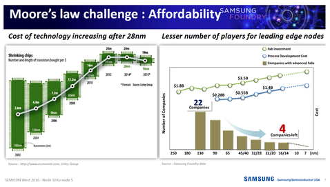
Our 2014 blog 28nm — The Last Node of Moore's Law has now been confirmed. At the time we wrote: “After the 28nm node, we can continue to make transistors smaller, but not cheaper.” It is illustrated in the following slide, presented by Samsung at the recent Semicon West 2016.
This discussion seems academic now, as the actual engineering costs of devices in advanced nodes have shown themselves to be too expensive for much of the industry. Consequently, and as predicted, the industry is bifurcating, and few products pursue scaling to 7nm while the majority of designs use 28nm or older nodes.
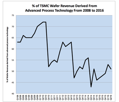
The following chart derived from TSMC quarterly earnings reports was published last week by Ed Sperling in the blog Stepping Back From Scaling:
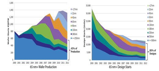
Similar industry dynamic has also been shown in a blog by MentorEstablished Technology Nodes: The Most Popular Kid at the Dance. Key quote:
“designs at 65 nm and larger still account for approximately 43% of all wafer production and 48% of wafer fab capacity. Even more significant, nodes 65nm and larger account for approximately 85% of all design starts (see charts below, source: VLSI Research). Clearly, established nodes are not fading away any time soon.”
A good conference to learn more about these new scaling technologies is the IEEE S3S ’16, held in the Hyatt Regency San Francisco Airport, October 10th thru 13th, 2016. CEA Leti is scheduled to give an update on their CoolCube program, Qualcomm will present some of their work on monolithic 3D, and three leading researchers from imec, MIT, and Korea universities collaboration will present their work on advanced monolithic 3D integration technologies, and many other authors will discuss their work on monolithic 3DIC and its ecosystem, in addition to tracks focused on SOI, sub-VT and dedicated sessions on IoT.


 RSS Feed