The Path to Alternative Scaling is Now Open

|
We have a guest contribution from Zvi Or-Bach, the President and CEO of MonolithIC 3D Inc.
IEEE S3S 2015 could be the turning point for monolithic 3D. During Oct. 4-7 we will have the option to get a short course, invited and selected presentations from a broad range of the industry representatives. They include major vendors such as Qualcomm, Global Foundries and Applied Materials; leading research organization like CEA Leti, Taiwan National Applied Research Labs, German IMS Chips, NASA; leading Universities like Berkeley and Stanford; start-ups like SiGen and MonolithIC 3D. |
IEEE S3S 2015 could be the turning point for monolithic 3D. During Oct. 4-7 we will have the option to get a short course, invited and selected presentations from a broad range of the industry representatives. They include major vendors such as Qualcomm, Global Foundries and Applied Materials; leading research organization like CEA Leti, Taiwan National Applied Research Labs, German IMS Chips, NASA; leading Universities like Berkeley and Stanford; start-ups like SiGen and MonolithIC 3D.
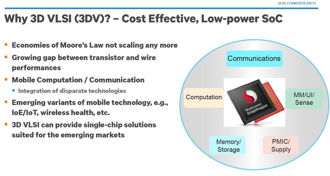
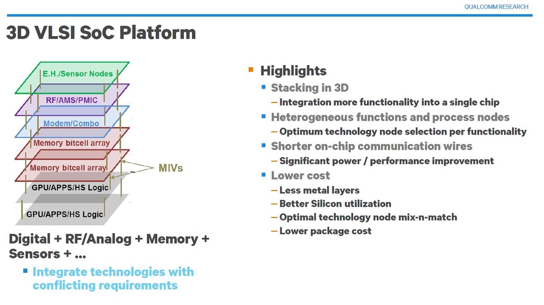
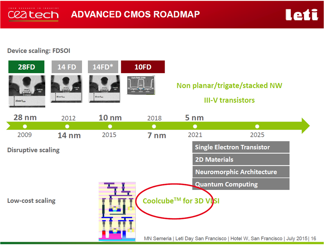
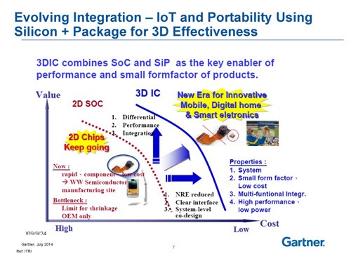
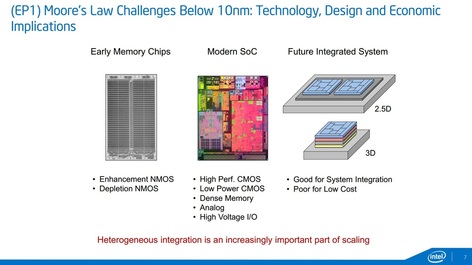
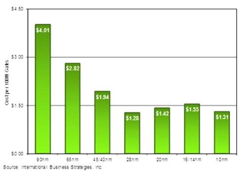
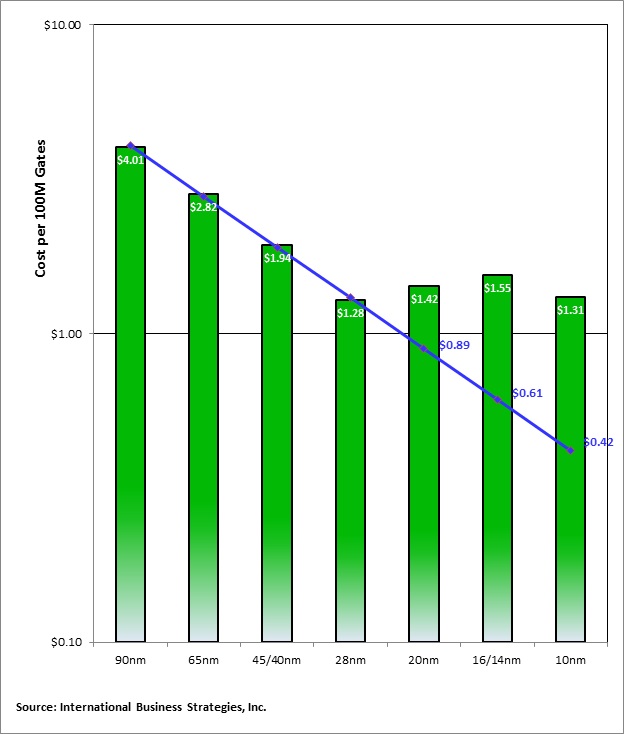
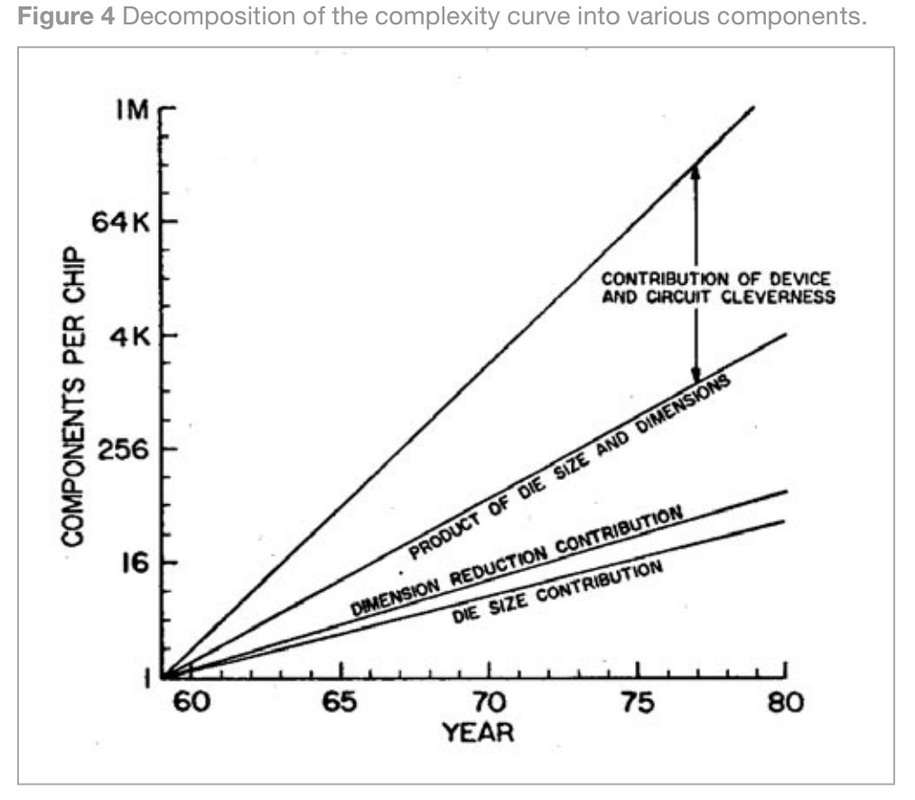
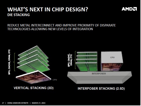
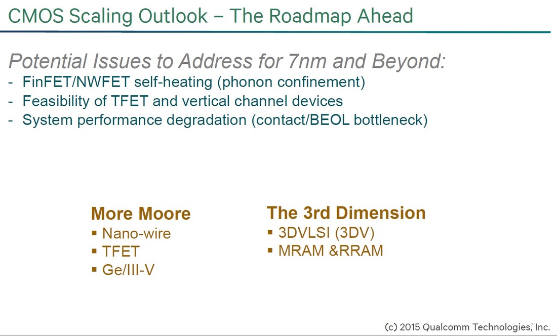
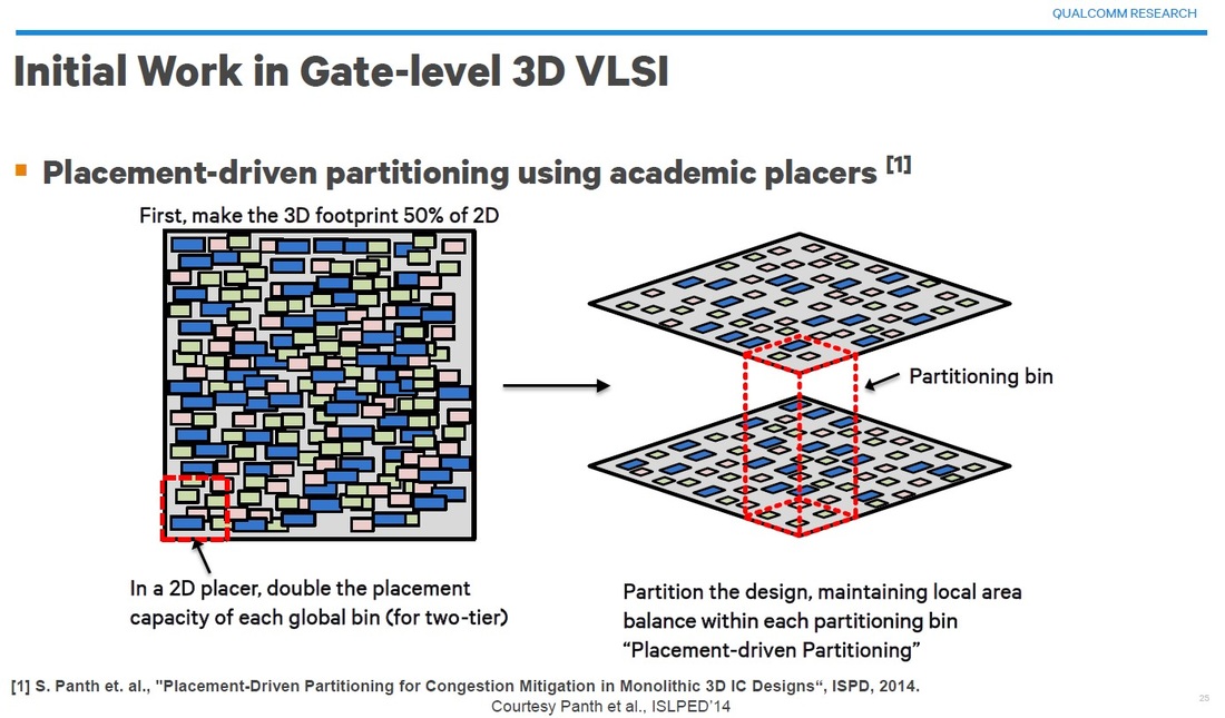
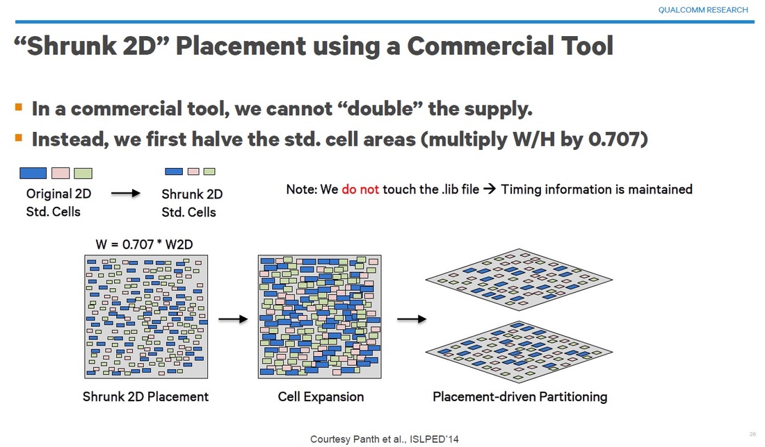
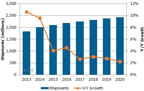
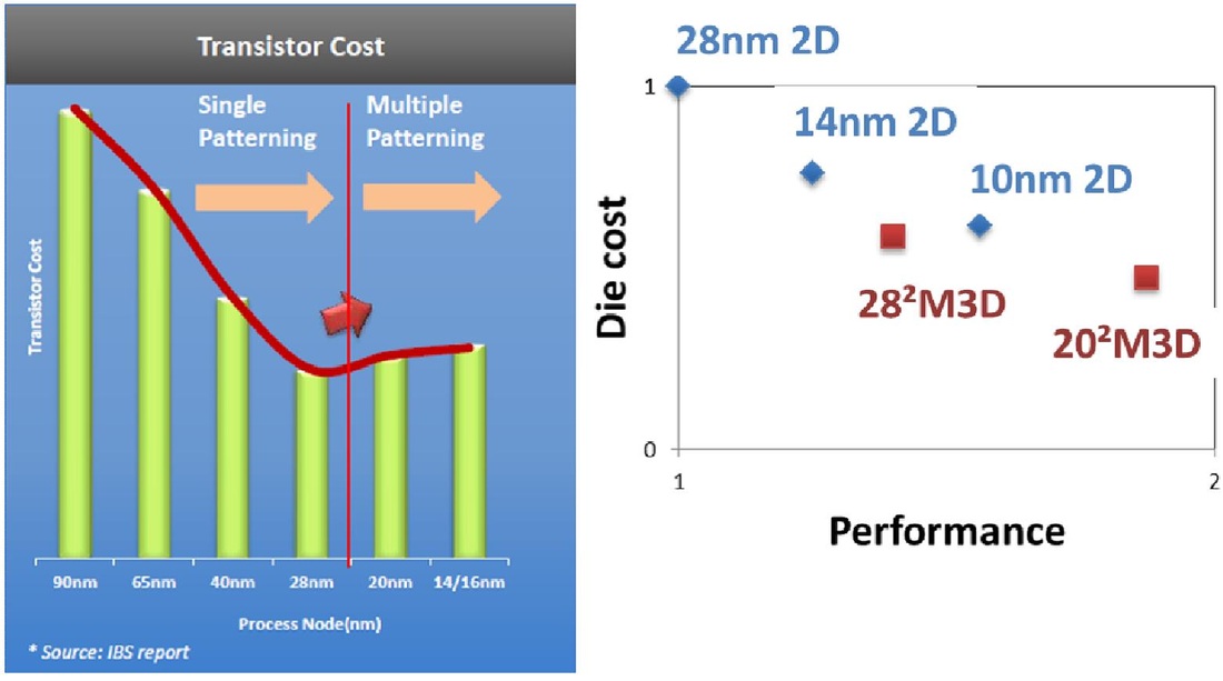
In its tutorial session Qualcomm will explain why it is investing and promoting 3D VLSI (3DV) as an alternative scaling technology, as is illustrated by the following two slides:
In its tutorial session Qualcomm will explain why it is investing and promoting 3D VLSI (3DV) as an alternative scaling technology, as is illustrated by the following two slides:
Yet many people still have doubts as is reflected by the title of the panel we were invited to participate in -- “Monolithic 3D: Will it Happen and if so…” -- at the IEEE 3D-Test Workshop Oct. 9, 2015.
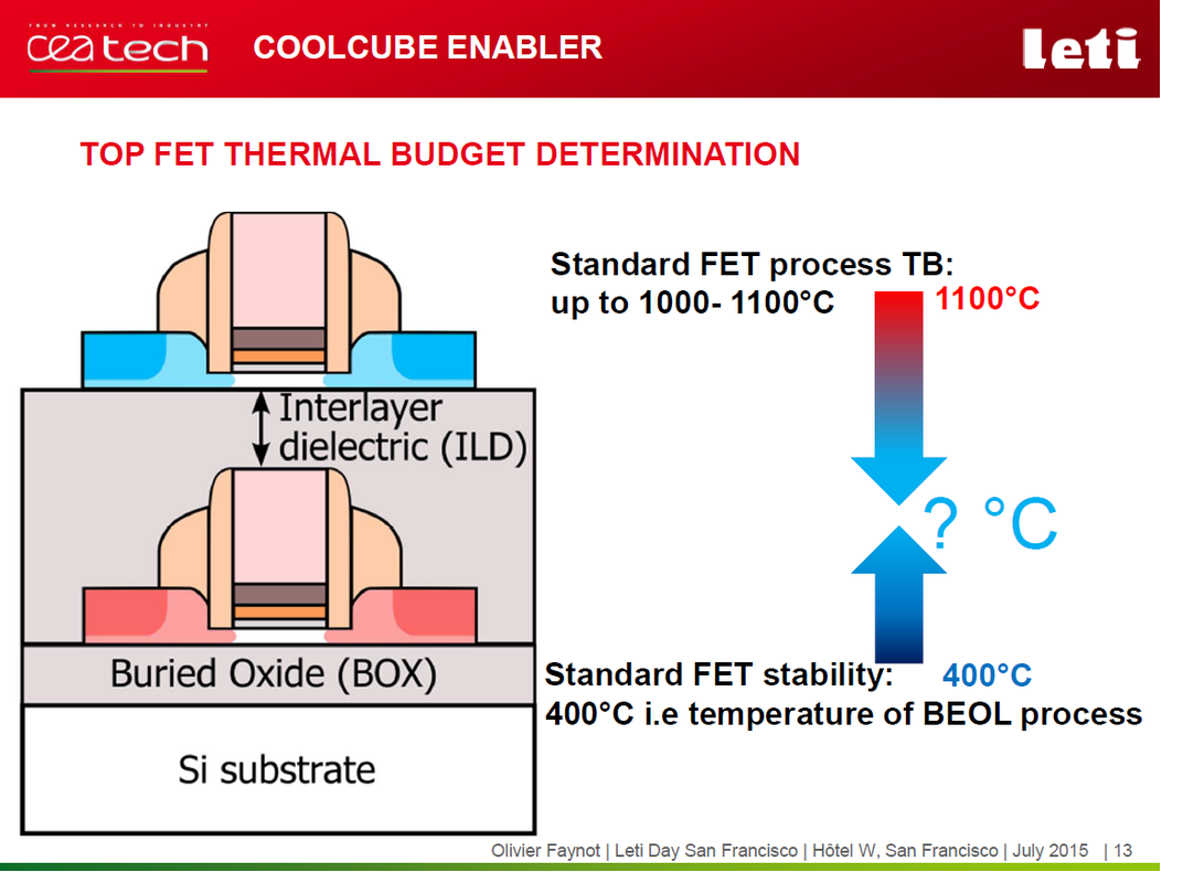
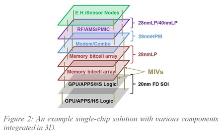
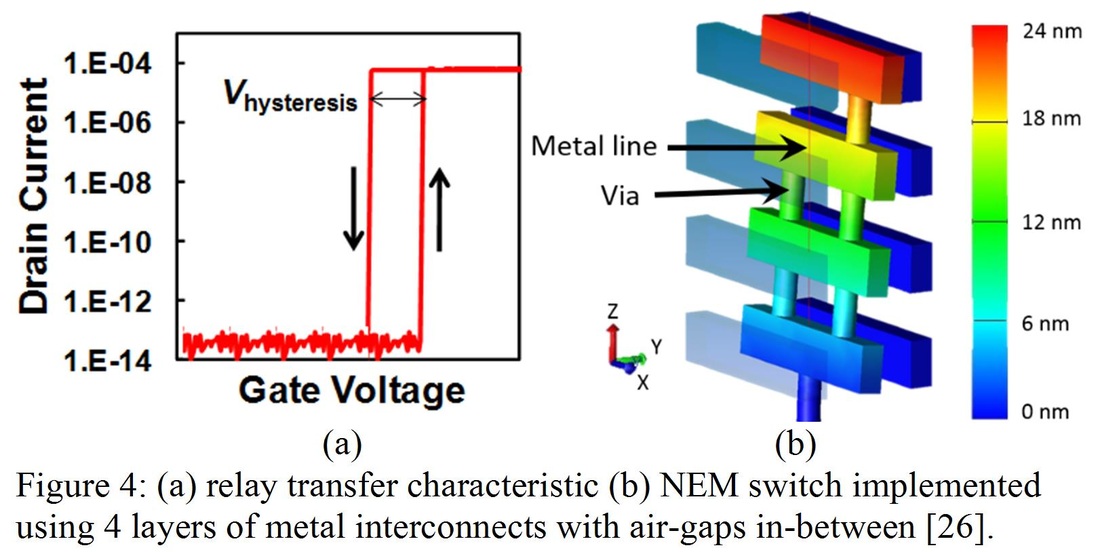
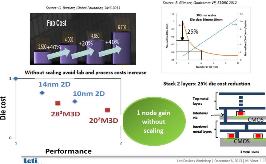
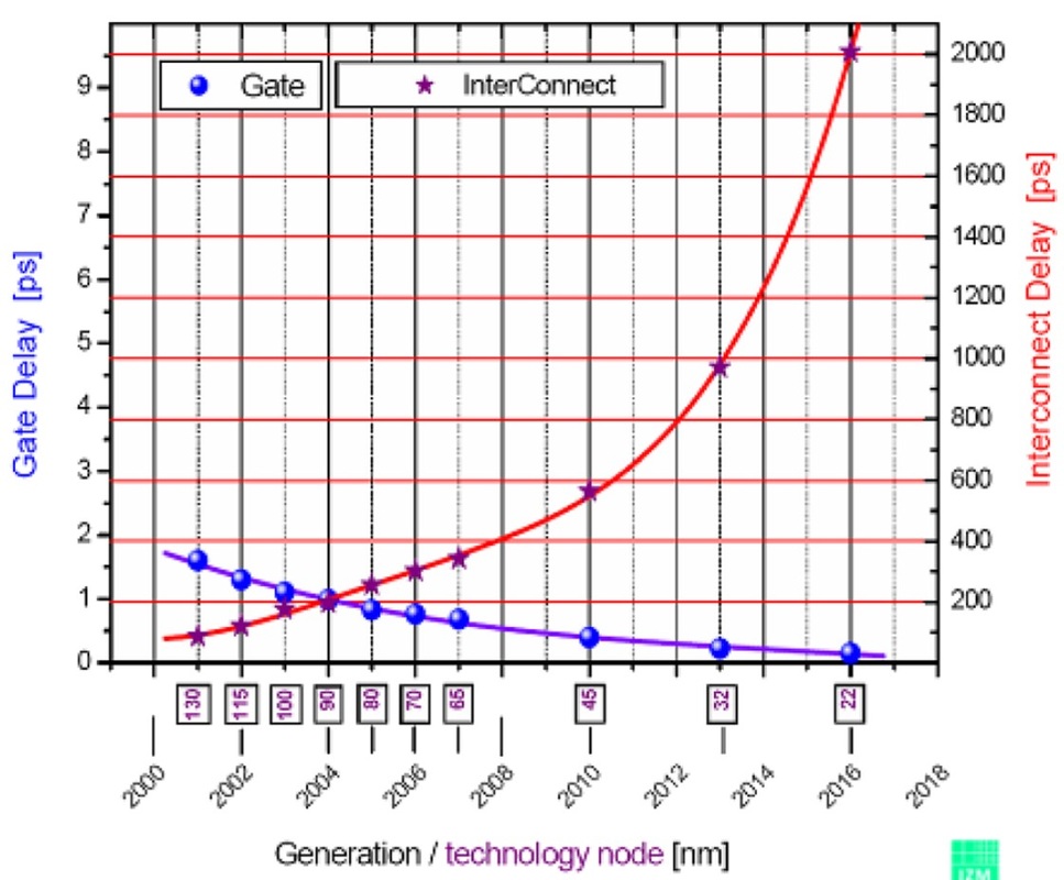
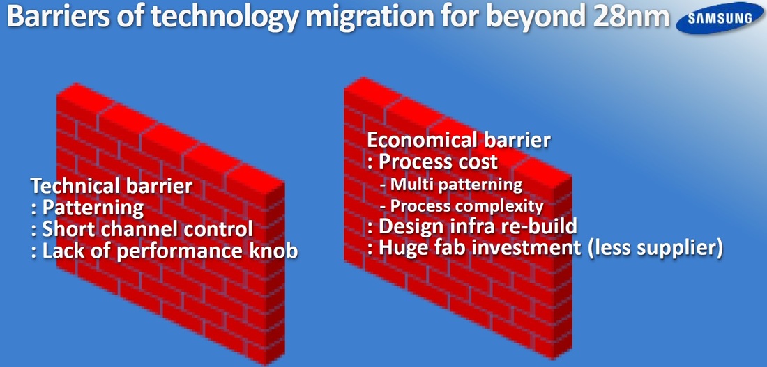
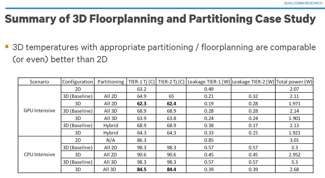
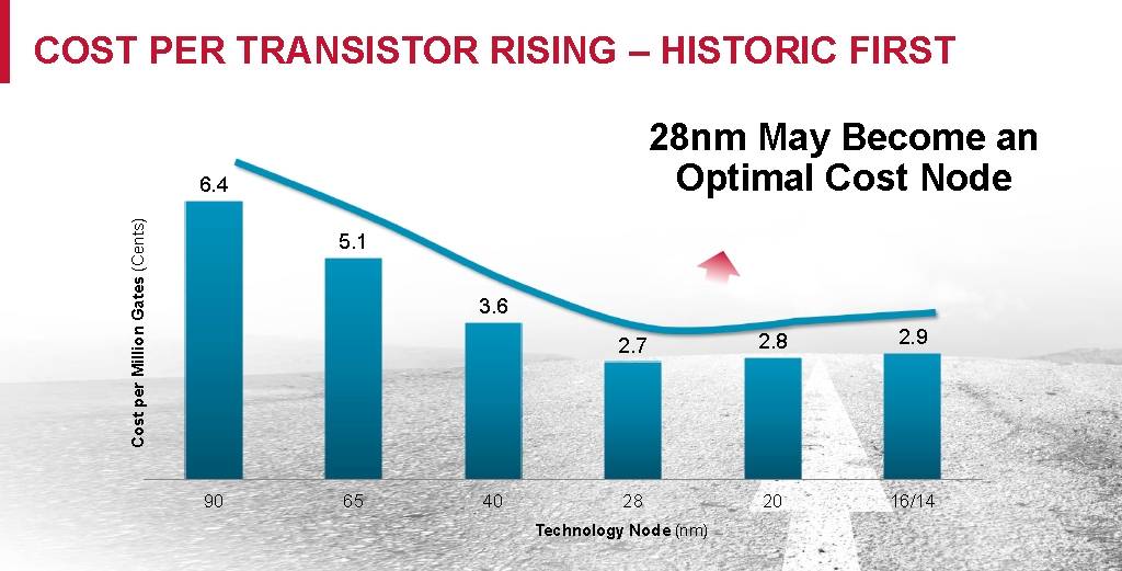
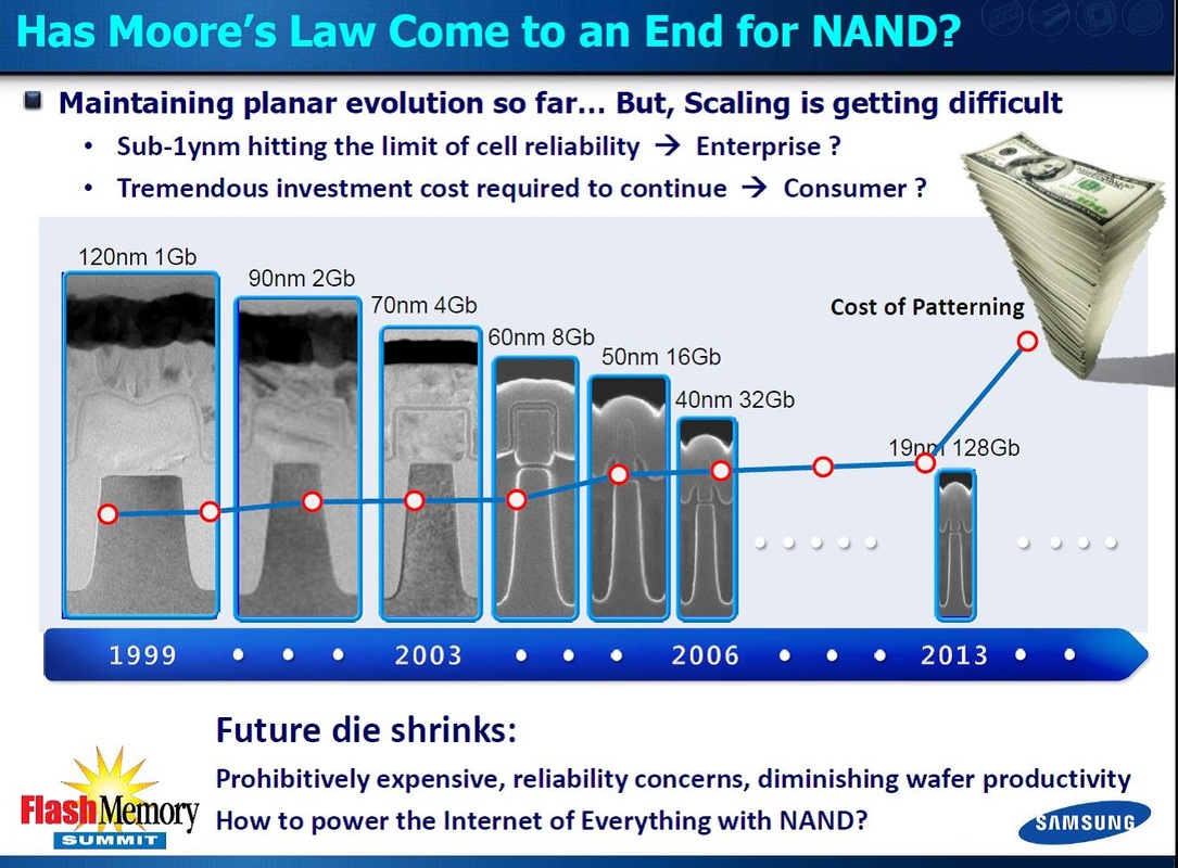
The doubts likely relate to the technology challenge that is illustrated in the following slide:
The doubts likely relate to the technology challenge that is illustrated in the following slide:
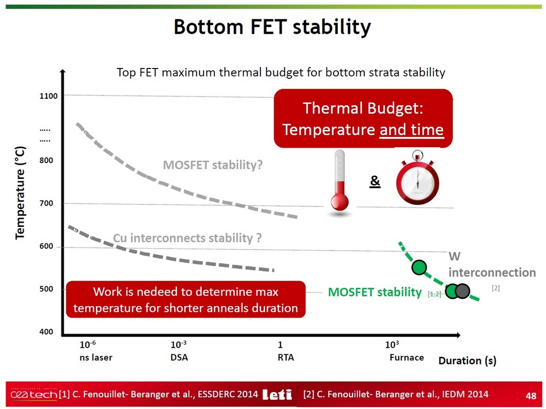
The question, in short, is how we can add more transistors monolithically interconnected to the underlying transistors without exceeding the thermal budget for the underlying transistors and interconnect.
The current paths to monolithic 3D involve major changes to the front line process flow and require the development of a new logic transistors. The big concern is that leading edge vendors are too busy with dimensional scaling and if anything else could be done it seems that FD-SOI would be it, while trailing edge fabs are, in most cases, avoiding any major transistor process development. The recent failure of Suvolta could be an indication of this reality.
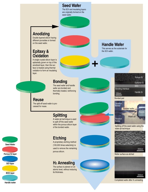
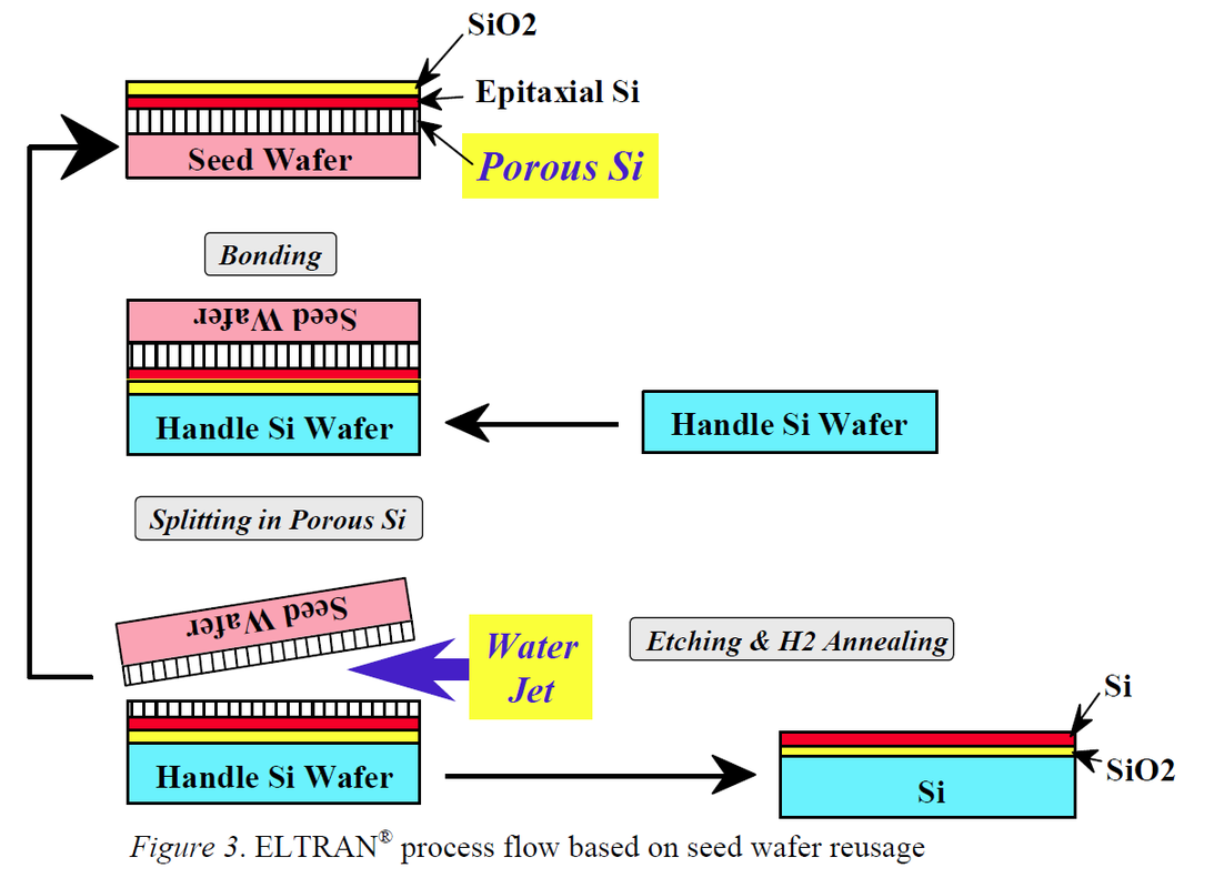
Hence the importance of Game-Changing 2.0, a major technology innovation to be unveiled on Wednesday by MonolithIC 3D in a paper titled: “Modified ELTRAN® - A Game Changer for Monolithic 3D”. The paper will present a novel use of the ELTRAN® process developed by Canon about 20 years ago primarily for SOI applications. Using ELTRAN (Epi. Layer Transfer) techniques, a substrate could be prepared enabling any fab to simply integrate a monolithic 3D device without the need to change its current front-line fab process. This flow is further simplified and could be integrated with the monolithic 3D flow introduced last year that leverages the emerging precision bonders, such as EVG’s GeminiÒ XT FB. This flow provides a natural path for product innovation and an unparalleled competitive edge to its adopters. In addition, this game-changing breakthrough offers a very cost-competitive flow. The following chart illustrates the original use of ELTRAN process for the fabrication of SOI wafers:
The current paths to monolithic 3D involve major changes to the front line process flow and require the development of a new logic transistors. The big concern is that leading edge vendors are too busy with dimensional scaling and if anything else could be done it seems that FD-SOI would be it, while trailing edge fabs are, in most cases, avoiding any major transistor process development. The recent failure of Suvolta could be an indication of this reality.
Hence the importance of Game-Changing 2.0, a major technology innovation to be unveiled on Wednesday by MonolithIC 3D in a paper titled: “Modified ELTRAN® - A Game Changer for Monolithic 3D”. The paper will present a novel use of the ELTRAN® process developed by Canon about 20 years ago primarily for SOI applications. Using ELTRAN (Epi. Layer Transfer) techniques, a substrate could be prepared enabling any fab to simply integrate a monolithic 3D device without the need to change its current front-line fab process. This flow is further simplified and could be integrated with the monolithic 3D flow introduced last year that leverages the emerging precision bonders, such as EVG’s GeminiÒ XT FB. This flow provides a natural path for product innovation and an unparalleled competitive edge to its adopters. In addition, this game-changing breakthrough offers a very cost-competitive flow. The following chart illustrates the original use of ELTRAN process for the fabrication of SOI wafers:
In the “Invited Talks on M3DI” at the conference we will have an opportunity to learn from the inventor of the ELTRAN process, Dr. Takao Yonehara, currently with Applied Materials, in his “Epitaxial Layer Transfer Technology and Application” talk. Prior to Applied Materials Dr. Yonehara worked with Solexel, a Silicon Valley startup, to deploy the ELTRAN process for low cost solar cell fabrication. Yonehara’s talk will be followed by Prof. Joachin Burghartz of Institute for Microelectronics in Stuttgart, discussing “Ultra-thin Chips for Flexible Electronics and 3D ICs” that uses a variation of such flow in small scale production.
The semiconductor industry is bifurcating these days into a segment that follows aggressive scaling for few super-value applications supported by very few vendors, while the bulk of the industry is enhancing old fabs targeting mainstream applications and the emerging IoT opportunities. Further enhancing these older fabs with monolithic 3D offers a most effective return on investment. Game-Changing 2.0 means that without a need for major process R&D efforts or new equipment, the path for 3D scaling is now open with enormous advantages for IoT. Accordingly, my answer to the original question above is summarized by the title of our invited talk at the IEEE 3D-Test Workshop:“Monolithic 3D is Already Here – the 3D NAND – and Now it would be Easy to Adapt it for Logic.”
In addition the other division – SOI and SubVt provide good complementing technology updates for the power-performance objectives that are so important for these emerging markets.
Do come to the S3S and enjoy unique key technologies update with the great wine and country pleasures of Sonoma Valley.


 RSS Feed