Embedded SRAM Scaling is Broken and with it Moore's Law

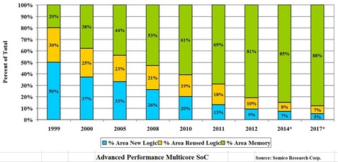
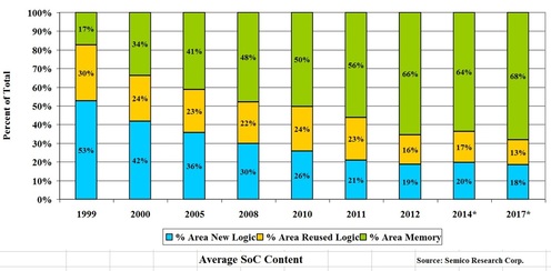
The percent of the die area used for embedded SRAM is growing with scaling and already exceeds 50%. The following two charts from Semico, which were recently updated, illustrates this for an advanced SoC and the average SoC
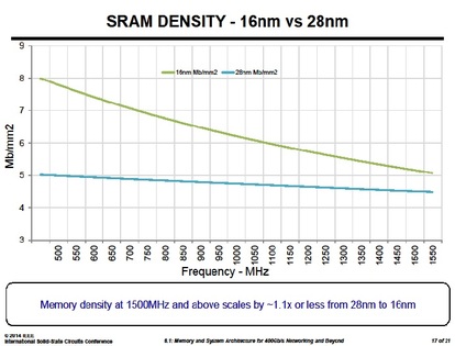
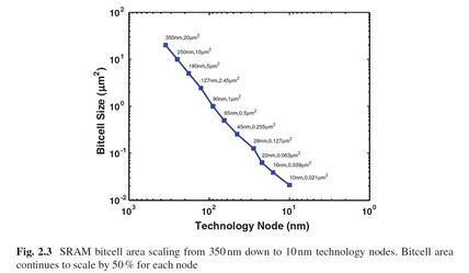
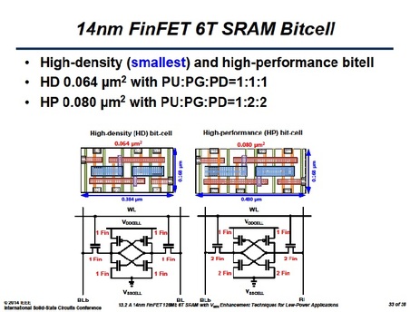
The above chart was about right all the way to 28nm, but scaling has broken since then. Already at 22/20 nm node the best bitcell size was about 0.09µm². But as TSMC reported at IEDM 2013 their bitcell for 16nm is 0.07µm². And now at ISSCC2014, Samsung presented similar results for 14nm FinFet as shown in the slide below.
This does not even take into consideration die size impacts required for implementing a new technology such as FinFETs. In their ISSCC 2014 paper, Samsung identified complications involved with the transition from Planar to finFET transistors including quantized width, strong PMOS and a lack of the body bias effect. Samsung disclosed a die size impact of 0.87% in order to add a Disturbance Noise Reduction (DNR) scheme to deal with the large more stable High Performance (HP) bit-cell. Samsung did not disclose the area impact of their proposed Negative Bitline write assist scheme used with their high density HD bit-cell but we can probably assume it is most likely significantly larger than the proposed scheme for the HP bit-cell.
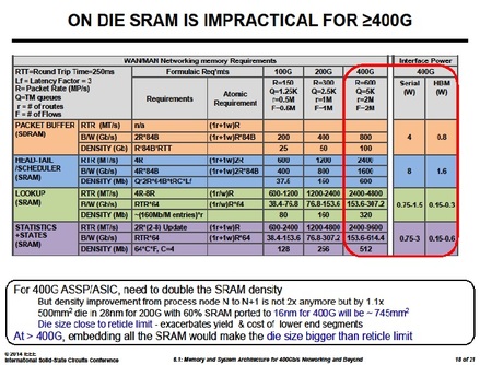
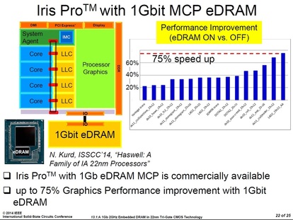
It is not too surprising to see the following slide presented by Intel at ISSCC 2014.
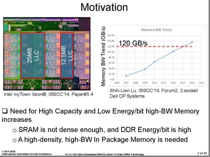
We can see from the following slide from ISSCC 2014 their motivation for adding the off chip embedded eDRAM is based on their need for a higher bandwidth Memory. Clearly SRAM scaling is not satisfying their requirements as they state “A high-density, high BW In Package Memory is needed.”
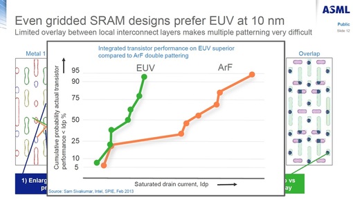
A. Lithography, the continuous delays in EUV force the industry to keep pushing with double and quad processes. The following chart by ASML illustrates the limitation effects on SRAM scaling:
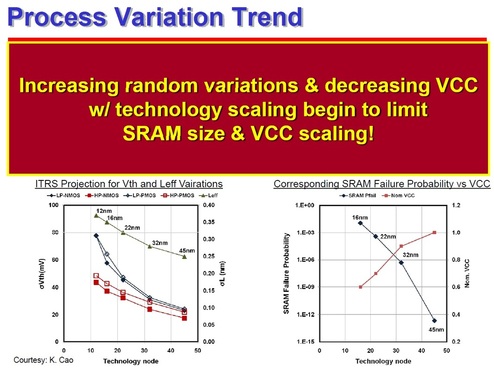
C. Decreasing VCC
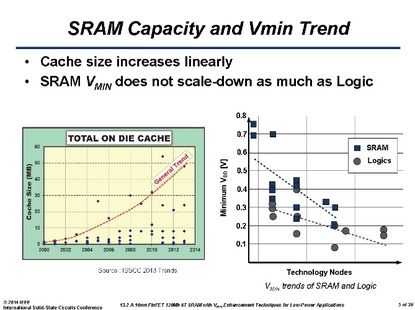
As seen in the above slide, and the slide presented by Samsung below, the trend is definitely clear. The minimum Vdd require to operate SRAM (Vmin) is not scaling as fast as the Vdd in the rest of the logic on die.
Bitcell scaling is getting harder, much harder, and even more so is the ability to scale large bocks of embedded SRAM. Adding to that the trend of growing the amount of embedded memory faster than the amount of logic cells and one could predict dark clouds for SoC scaling beyond 28nm. It seems that brute-force scaling is not practical anymore but two technology innovation breakthroughs could solve the SRAM memory scaling problem and provide a scalable high density memory if adopted soon by the industry.
The first innovation is the 1 Transistor SRAM (1T SRAM) developed by Zeno Semiconductor. This 1T SRAM, utilizes existing fab process and provides a 90% bitcell size reduction vs. conventional 6T SRAM and will keep scaling beyond 28nm.
The second is monolithic 3D, which enables a very effective heterogeneous integration scheme, allowing for the SRAM layer to be optimized for memory while the logic layer could be optimized for logic - Monolithic 3D eDRAM on Logic
The most expensive SRAM in the world doesn’t need to come to pass



 RSS Feed