
We have a guest contribution today from Israel Beinglass, the CTO of MonolithIC 3D Inc. Israel talks about the use of monolithic 3D integration for SRAM stacking above/below logic.
When people are talking about 3D devices, they are most likely referring to TSV.
What is the “killer application” of TSV? Well, it depends on who do you ask. Is it DRAM stacking? Or is it DRAM on top of a Microprocessor, or logic stacking, or FPGA on Silicon - passive interposer (2.5D)? However, as of now, it looks like very few things shown in "3D roadmaps" have happened.
According to Yuan Xie of Penn. State University who specializes in 3D architecture design, for 3D IC to be adopted, it has to both enable novel architecture as well as identify a killer application. Things such as latency improvement, better bandwidth, integration and cost benefits are what will make 3D IC happen.
At this point I’d like to make a detour and bring to your attention an even better application for 3D-IC using the monolithic 3D approach. But before that I’d like to ask all of you the following question.
Question: what is the most expensive SRAM in the world?
Answer: Any microprocessor containing SRAM Cache, e.g. Intel’s Penryn 45nm processor or the like (http://www.legitreviews.com/article/480/1/ , see Figures 1 and 2)
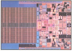
Figure 1: The Intel Penryn Chip
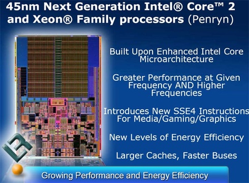
Figure 2: The benefits of the Penryn microprocessor
By looking at the chip layout, it is clear that half of the area is SRAM cache. So, if you consider the price that the user pays for the chip, the price per unit area of SRAM is unbelievably high!!!
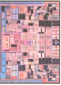
Figure 3: The "logic" part (left) and the cache part (right)
Now look at these two chip parts shown in Figure 3. What happens If we put them one on top of the other and interconnect them through “real vias’” and not using the problematic low-density TSV technology - wouldn’t it be wonderful?
Let’s look at the benefits of separating these two chips and using the MonolithIC 3D technology involving layer transfer.
1. Each chip is much smaller than the original chip size i.e. the yield will be higher on each chip (of course some design modifications need to be done)
2. The “logic” part could be optimizing as a separate chip and at the same time the SRAM could be optimized by itself.
3. The number of metal layers is drastically different, in the logic chip 8-10 metal layers are needed while in the SRAM probably no more than 3 layers are needed. Hence, we get a much better utilization of chip production.
4. The interconnect between the SRAM and the logic part is much shorter along the vertical direction vs. the horizontal (planar) direction.
In summary, this example of a highly SRAM populated chip that could be divided into two chips with a MonolithiIC 3D integration method just makes sense.


 RSS Feed