
We have a guest contribution today from Brian Cronquist, MonolithIC 3D Inc.'s VP of Technology & IP. Brian discusses why he believes Monolithic 3D-IC could be less risky than scaling or TSV.
I recently saw this great 5 minute video by Applied Material’s Richard Lewington [AMAT 3D Blog Video] where three types of 3D-IC construction are demonstrated. Note that the first two 3D-IC options he shows (with those plastic blocks) are monolithic. Only the third option is TSV based.
What’s going on here? Why is this major equipment vendor talking about monolithic 3D when it seems that most of what the industry is talking about these days are scaling, interposers, and Thru-Silicon-Vias(TSVs)? Let’s take a look.
Being a fab-guy (built parts of and worked in Chartered Fab-1 & Fab-2, Sierra Semi’s fab inside National Semi’s Bldg#4, AMI Poci Fab-4, Synertek Fab-3, etc.) I am going to approach this from a process/fab-rat perspective. Because this is a key point to what monolithic 3D is about: it is supposed to bring 3D-IC back into the wafer batch economics of semiconductor processing. No piece part handling expense, TSV/interposer reliability & cost issues, or OSAT troubles (I applaud TSMC for trying to remedy this OSAT part, but am surprised that Global Foundries did not do it first….they could have beaten TSMC to the punch here).
The major rule for wafer fabs is Take no Risks….. Everything you do is focused on control: understanding, eliminating, controlling variables. Protect and preserve that huge capital investment so you can pay it down. By definition & nature, fab managers are very conservative. But scaling forced us to do dramatically different and risky things. That’s a major reason why it takes 10+ years for new process/technologies to get into a large production fab. Think about HKMG, Cu BEOL, CMP, strain, plasma metal etching rather than wet (caused lots of corrosion issues/mousebites), to name a few. Even platen cooling (instead of aluminum mask layers) for high current implantation took a long time. Changing from flats on the starting material wafers to the notch took about 10yrs too.
At its root, many of these changes took new machines, new chemistries, and/or new process methods (think APCVD, LPCVD, UHVCVD, PECVD, SACVD, ALCVD, MOCVD, RTCVD, …..) Another large risk factor with scaling has been the use of more elements of the periodic table to solve scaling challenges. We did not just alter the form or compound of a known element (bad enough risk-wise); we changed to and added new elements to our expensive wafer fabs. (In fab parlance, all this “newness†added up to what is called the Sphincter Effect)
When I started in the industry we used only six elements from the periodic table:
What’s going on here? Why is this major equipment vendor talking about monolithic 3D when it seems that most of what the industry is talking about these days are scaling, interposers, and Thru-Silicon-Vias(TSVs)? Let’s take a look.
Being a fab-guy (built parts of and worked in Chartered Fab-1 & Fab-2, Sierra Semi’s fab inside National Semi’s Bldg#4, AMI Poci Fab-4, Synertek Fab-3, etc.) I am going to approach this from a process/fab-rat perspective. Because this is a key point to what monolithic 3D is about: it is supposed to bring 3D-IC back into the wafer batch economics of semiconductor processing. No piece part handling expense, TSV/interposer reliability & cost issues, or OSAT troubles (I applaud TSMC for trying to remedy this OSAT part, but am surprised that Global Foundries did not do it first….they could have beaten TSMC to the punch here).
The major rule for wafer fabs is Take no Risks….. Everything you do is focused on control: understanding, eliminating, controlling variables. Protect and preserve that huge capital investment so you can pay it down. By definition & nature, fab managers are very conservative. But scaling forced us to do dramatically different and risky things. That’s a major reason why it takes 10+ years for new process/technologies to get into a large production fab. Think about HKMG, Cu BEOL, CMP, strain, plasma metal etching rather than wet (caused lots of corrosion issues/mousebites), to name a few. Even platen cooling (instead of aluminum mask layers) for high current implantation took a long time. Changing from flats on the starting material wafers to the notch took about 10yrs too.
At its root, many of these changes took new machines, new chemistries, and/or new process methods (think APCVD, LPCVD, UHVCVD, PECVD, SACVD, ALCVD, MOCVD, RTCVD, …..) Another large risk factor with scaling has been the use of more elements of the periodic table to solve scaling challenges. We did not just alter the form or compound of a known element (bad enough risk-wise); we changed to and added new elements to our expensive wafer fabs. (In fab parlance, all this “newness†added up to what is called the Sphincter Effect)
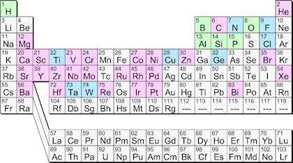
When I started in the industry we used only six elements from the periodic table:
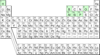
Here is the current periodic table usage:
Yet, all of us scientists and engineers, as well as fab managers, solved the problems caused by relentless scaling, and the industry grew…we had a lot of fun, we were supremely challenged, and we solved those challenges. But we also grew grey hair and permanently pinched sphincters.
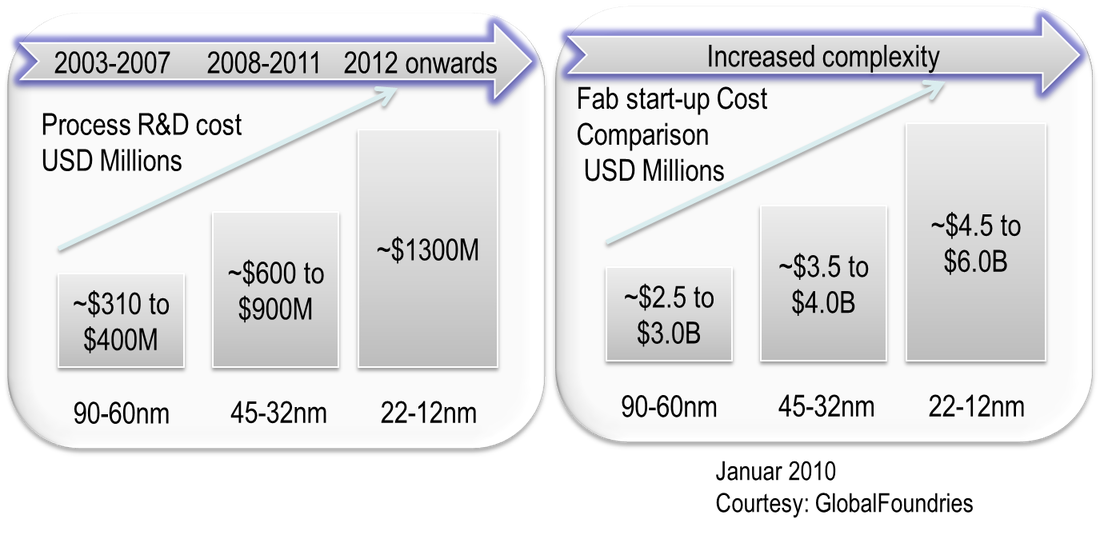
At what cost? (remember, low cost is crucial to successful manufacturing!)
Here’s what Global Foundries showed about costs:
At what cost? (remember, low cost is crucial to successful manufacturing!)
Here’s what Global Foundries showed about costs:
So, now we have now included the investment and banking communities into our Sphincter Effect.:-))
Enough! This is the road to ruin; well, at least to vastly diminishing returns (think Handel Jones’ chart [ElectroIQ link to ISS12 Day 2] on how transistor cost is no longer going down…)
3D-IC is the solution. OK, so…. monolithic or TSV or interposer? Above I already mentioned a few of the risks and costs to a TSV/interposer solution. Look at all the new processes and machines that had to be developed to etch and fill such deep holes at least somewhat economically. And the integration issues are significant because of the novelty and the architecture & flow: Cu/silicon stresses, keep out zones, liners, new reliability fail modes, etc. As usual, these issues will likely be solved; hence, TSV & interposers will be useful for obtaining some cost and functional/architectural gains from its limited vertical connectivity. But they are not the endgame. To get fully back onto the economic scaling path we need rich vertical connectivity.
What about monolithic 3D-IC risks & costs? Fab equipment and unit processes exist. No new elements from the periodic table are necessary. And the gains resulting from this dense vertical connectivity keep us on a scaling equivalent path (no need to spend space here…lots has been written about this). Let’s instead look at the process details:
Oxides for ox-ox direct bonding: Deposited oxides are well understood and cheap. No new equipment or elements are needed. Lots of manufacturing proven techniques to get there: PECVD, SACVD, etc.
H Implant: Can be done on current models. No new equipment needed. Done by SOI manufacturers for 20 years. H in silicon is well understood.
Bonding: Two well-known equipment vendors (EVG & SUSSMicroTec) with low temp oxide to oxide bonding capability and significant sales of machines (mostly to BSI sensor folks at this time). A recent third new entry (MHI-Mitsubishi Heavy Industries) with room temp ox-ox bonding. I recently blogged on this topic too. [BC LT direct bonding]
Cleave: Lots of methods proven for SOI manufacture, sensors, and solar. Simplest is thermal … just use a furnace or RTP. We made a short movie clip showing how simple cleave is with the AG RTP at Stanford.
Monolithic 3D-IC uses existing wafer-fab equipment, needs no new elements from the periodic table, and utilizes well-known unit processes and chemistries.
What’s the catch? It’s the integration. Integration work (blood, sweat, and tears) will always be there, even with no new elements, machines, chemistries, etc. Always. However, those who have done new process introductions know that integration is significantly less risky (= costly) and faster to market without than with the elements/machine/chemistry changes. New modes of defect generation are always generated from integration, but there are a lot less of them if all the unit processes are standard accepted practices, than if those unit processes are totally new.
If you look very very carefully at the MonolithIC 3D Inc’s process flows, you notice we were single mindedly focused on making it simple. For example, the nm-scale thru layer vias (TLVs) are always made thru the STI (Shallow Trench Isolation); hence, no dielectric liners, minimum stress, conventional etch and fill, nothing high aspect ratio about it. Make the TLV look and feel like a regular metal to metal via.
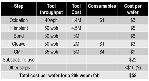
This shows in the costs. Deepak Sekar did a SEMATECH based cost estimate and talked about it in a blog. [Deepak Blog ion-cut cost] Here’s his summary chart for 300mm wafers.
Enough! This is the road to ruin; well, at least to vastly diminishing returns (think Handel Jones’ chart [ElectroIQ link to ISS12 Day 2] on how transistor cost is no longer going down…)
3D-IC is the solution. OK, so…. monolithic or TSV or interposer? Above I already mentioned a few of the risks and costs to a TSV/interposer solution. Look at all the new processes and machines that had to be developed to etch and fill such deep holes at least somewhat economically. And the integration issues are significant because of the novelty and the architecture & flow: Cu/silicon stresses, keep out zones, liners, new reliability fail modes, etc. As usual, these issues will likely be solved; hence, TSV & interposers will be useful for obtaining some cost and functional/architectural gains from its limited vertical connectivity. But they are not the endgame. To get fully back onto the economic scaling path we need rich vertical connectivity.
What about monolithic 3D-IC risks & costs? Fab equipment and unit processes exist. No new elements from the periodic table are necessary. And the gains resulting from this dense vertical connectivity keep us on a scaling equivalent path (no need to spend space here…lots has been written about this). Let’s instead look at the process details:
Oxides for ox-ox direct bonding: Deposited oxides are well understood and cheap. No new equipment or elements are needed. Lots of manufacturing proven techniques to get there: PECVD, SACVD, etc.
H Implant: Can be done on current models. No new equipment needed. Done by SOI manufacturers for 20 years. H in silicon is well understood.
Bonding: Two well-known equipment vendors (EVG & SUSSMicroTec) with low temp oxide to oxide bonding capability and significant sales of machines (mostly to BSI sensor folks at this time). A recent third new entry (MHI-Mitsubishi Heavy Industries) with room temp ox-ox bonding. I recently blogged on this topic too. [BC LT direct bonding]
Cleave: Lots of methods proven for SOI manufacture, sensors, and solar. Simplest is thermal … just use a furnace or RTP. We made a short movie clip showing how simple cleave is with the AG RTP at Stanford.
Monolithic 3D-IC uses existing wafer-fab equipment, needs no new elements from the periodic table, and utilizes well-known unit processes and chemistries.
What’s the catch? It’s the integration. Integration work (blood, sweat, and tears) will always be there, even with no new elements, machines, chemistries, etc. Always. However, those who have done new process introductions know that integration is significantly less risky (= costly) and faster to market without than with the elements/machine/chemistry changes. New modes of defect generation are always generated from integration, but there are a lot less of them if all the unit processes are standard accepted practices, than if those unit processes are totally new.
If you look very very carefully at the MonolithIC 3D Inc’s process flows, you notice we were single mindedly focused on making it simple. For example, the nm-scale thru layer vias (TLVs) are always made thru the STI (Shallow Trench Isolation); hence, no dielectric liners, minimum stress, conventional etch and fill, nothing high aspect ratio about it. Make the TLV look and feel like a regular metal to metal via.
This shows in the costs. Deepak Sekar did a SEMATECH based cost estimate and talked about it in a blog. [Deepak Blog ion-cut cost] Here’s his summary chart for 300mm wafers.
Validation of Monolithic 3D
One may make the argument that validation of a nascent & new game-changing technology is impossible, or at least very nearly so. However, for monolithic 3D-IC there are at least two important data-points to consider. And I hope that you will be convinced that monolithic 3D-IC is neither so nascent nor new.
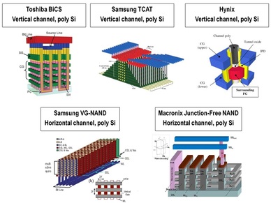
NAND Memory Makers going 3D: People such as David Lammers of Semiconductor Manufacturing & Design Community [Lammers July 2011] have pointed to validation evidence that the time of monolithic 3D-IC is near: the bleeding edge NAND memory makers are already moving to monolithic 3D-IC.
“The advent of 3D NAND memories may be only two or three years away, speakers said at Semicon West in San Francisco. By 2013 the major memory companies developing 3D NAND, including Hynix, Samsung, and Toshiba, may be ready with pilot lines, moving to volume production a year or so later. Taiwan-based Macronix International also has been developing a 3D NAND solution.â€
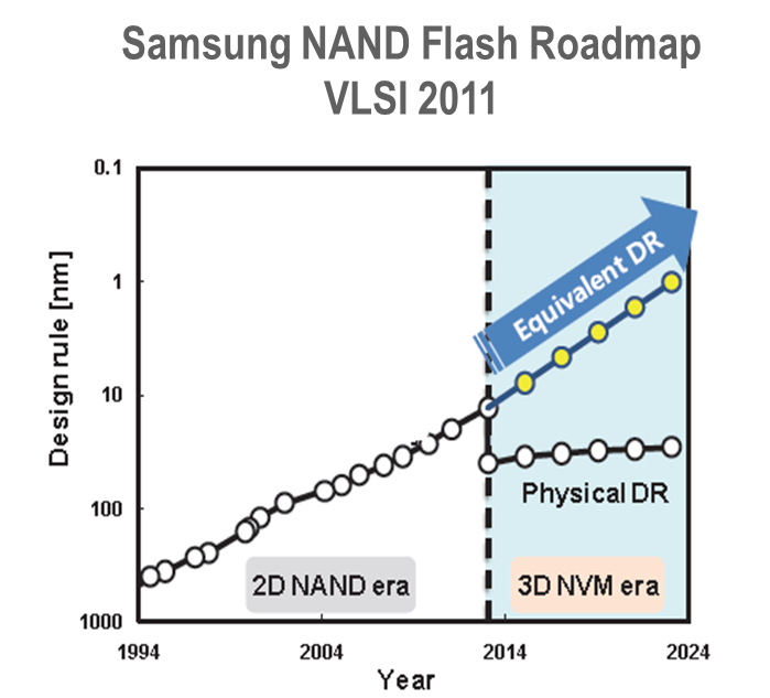
At the recent (2011) VLSI Symposium J. Choi of Samsung showed their view of how they will keep on making cheaper bits … by going 3D monolithically.
One may make the argument that validation of a nascent & new game-changing technology is impossible, or at least very nearly so. However, for monolithic 3D-IC there are at least two important data-points to consider. And I hope that you will be convinced that monolithic 3D-IC is neither so nascent nor new.
NAND Memory Makers going 3D: People such as David Lammers of Semiconductor Manufacturing & Design Community [Lammers July 2011] have pointed to validation evidence that the time of monolithic 3D-IC is near: the bleeding edge NAND memory makers are already moving to monolithic 3D-IC.
“The advent of 3D NAND memories may be only two or three years away, speakers said at Semicon West in San Francisco. By 2013 the major memory companies developing 3D NAND, including Hynix, Samsung, and Toshiba, may be ready with pilot lines, moving to volume production a year or so later. Taiwan-based Macronix International also has been developing a 3D NAND solution.â€
At the recent (2011) VLSI Symposium J. Choi of Samsung showed their view of how they will keep on making cheaper bits … by going 3D monolithically.
Deepak Sekar has also talked in detail about this 3D monolithic push by the NAND industry (Sekar hails from flash maker SanDisk) in his recent blog [12/11/2011: where-is-the-nand-flash-industry-heading].
Second, the global semiconductor equipment leader, AMAT, has talked about sales into that market [SemiconWest2011-new products including 3D architecture support]
[OptivaCVD for BSI] and even has a video (Richard Lewington’s blog video noted above) to promote it.
When both manufacturers and equipment suppliers are talking about, committing to, and executing on a specific technology change, you know that the economics are attractive and not just niche. Think back to how HKMG and copper BEOL came to production.
The chicken and egg are out the window….it’s happening now. The risks are contained. Others are going for it.
Whether polysilicon or monocrystalline silicon based monolithic 3D, jump in and be a part of this next important evolution of our great industry.
Don’t miss out.


 RSS Feed