
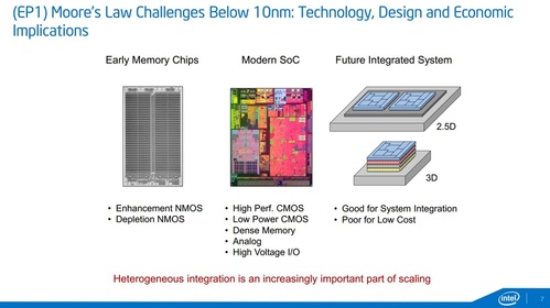
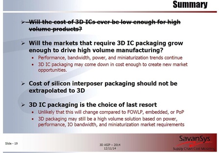
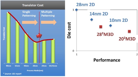
With respect to "Poor for Low Cost," this is only true for the TSV approach to 3D ICs. The following slide was presented in the recent 3D ASIP (2014) conference as the summary of "Will the Cost of 3D ICs Ever Be Low Enough for High Volume Products" presentation by Chest Palesko, a leading market researcher:
But the other form of 3D IC, the Monolithic 3D, is the lowest cost path for future scaling!
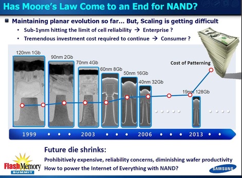
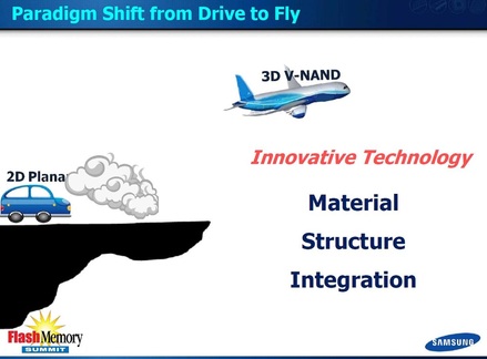
Samsung’s 3D NAND is an early example of monolithic 3D enabled scaling, being driven primarily by the push to increase bit capacity while reducing the cost per bit. Monolithically scaling up is now part of the ITRS and is being adopted by all NAND vendors. Samsung was the first to bring 3D NAND to mass production using the monolithic 3D approach:
While still in the R&D phase, there is momentum building for monolithic 3D in logic too, as reported by CEA Leti’s work in collaboration with ST Micro, IBM, and Qualcomm. This was presented in the S3S (2014), 3D ASIP (2014), and IEDM (2014) conferences. The following chart was presented by CEA Leti and shows the cost reduction and performance improvements enabled by monolithic 3D scaling:
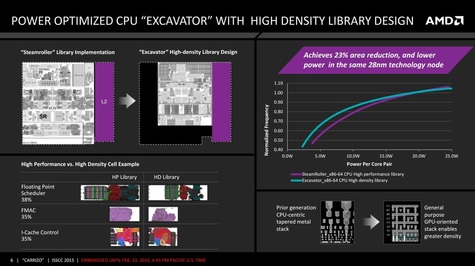
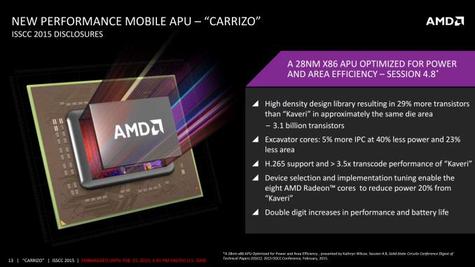
A misleading benefit which often gets attributed to dimensional scaling but has little to do with it, is the wide range of device improvements resulting from R&D efforts that typically coincide with the next scaling node. AMD’s recent presentation at ISSCC 2015 clearly illustrates this point by showing device improvements while still staying at the same 28 nm process node. As could be seen, major improvement in power, yield, and performance are possible over time without changing the technology node.
Until recently, the path to monolithic 3D required change to the front end-of-line process. An FEOL process change is always part of dimensional scaling, but is expensive, risky and in most cases done only by the leading edge companies. Now, as was presented in the recent IEEE S3S ‘14 conference, emerging precision bonders, such as from EVG or Nikon, enable a Game Changer for Monolithic 3D - a "true monolithic 3D IC without the need for a new recipe for transistor formation. The process could be adopted by any current fab providing very competitive costs for a range of product enhancements and offers a long term road map for better offerings by scaling up."
P.S.
A good conference to learn about this new scaling technology is the IEEE S3S ‘15, in Sonoma, on October 5th thru 8th, 2015. Two leading researchers from Berkeley and Stanford Universities will give invited talks presenting their work on advanced monolithic 3D integration technologies.



 RSS Feed