
We have a guest article today from Brian Cronquist, VP of Technology at MonolithIC 3D Inc. Brian has 30 years of global experience on “both sides of the silicon wafer table”: starting and building Chartered Semiconductor (Singapore) technology and customers as a captive then pure foundry, and non-volatile FPGA technology at Actel as a fabless partner and customer to over 7 foundries and IDMs. He discusses cost implications of Monolithic 3D.
An old CEO (John East of Actel) of mine kept drilling into our heads that “faster, cheaper, and easier to use” was the path to success in the IC industry, and that “Cheaper” was the key element of those three. Economics has always been a, maybe even the, key driver for scaling in specific [Moore's 1995 SPIE speech] and the industry in general.
So it was no surprise that when I have brought 3D-IC, and specifically monolithic 3D, into the potential solution space for combating the growing only-nations-can-afford-them costs of conventional (Dennard, etc.) scaling [IBM: Scaling dead], the first question out of their mouths (or keyboards) is: “Hey, doesn’t it cost twice as much to fold and stack it, so one gains nothing and perhaps even loses something due to the added costs of doing the 3D process (bonding, cleaving, connection)???” Well, when I started my monolithic 3D journey, I had the same first thoughts and questions. Here are a few of the answers….more will be forthcoming in future blogs and publications. Cost is a vast topic.
Die Size/Cost
“Hey, if I fold my chip over once, then I have the same silicon area (cost) as 2D but now double the processing, metal layers, etc., plus the costs of making and connecting the stack, right?” Well, that was my first impression too. But let’s take a deeper look. By placing about half the circuitry above the other half (i.e.: “folding”), not only do the long wires get shorter, but so does the average wire*. Hence, close to all of the logic gate to logic gate drivers and block to block buffers become smaller. Since they are smaller, then the circuitry moves closer to its neighbor; hence, the drivers can become smaller again. This positive feedback mechanism has been modeled by many people. Take a look at Davis, Zhou, and Synopsys, the references can be found at [Refs] as well as Meindl at MCISE 2003. This is a tractable problem for the universities, so there are many studies out there.
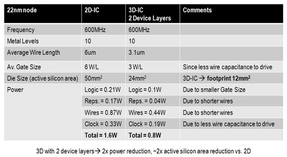
At Monolithic 3D Inc., we also have taken a close look at this to convince ourselves. Deepak took an older version of the IntSim tool he developed as part of his PhD thesis at Georgia Tech [Refs] and upgraded it to 3D. You will see more publications on this tool and results, and it will soon be available on our website for you to try [3DSim]. Here is one result: The baseline was a 600MHz low power 2D logic core constructed at 22nm. A more complete description is at [Why Monolithic 3D], but the bottom line is: The monolithic 3D IC footprint is one fourth the die size of the 2D, and the total silicon area of the 3D chip is slightly less than half of the 2D chip (24 sq. mm vs 50 sq. mm).
So it was no surprise that when I have brought 3D-IC, and specifically monolithic 3D, into the potential solution space for combating the growing only-nations-can-afford-them costs of conventional (Dennard, etc.) scaling [IBM: Scaling dead], the first question out of their mouths (or keyboards) is: “Hey, doesn’t it cost twice as much to fold and stack it, so one gains nothing and perhaps even loses something due to the added costs of doing the 3D process (bonding, cleaving, connection)???” Well, when I started my monolithic 3D journey, I had the same first thoughts and questions. Here are a few of the answers….more will be forthcoming in future blogs and publications. Cost is a vast topic.
Die Size/Cost
“Hey, if I fold my chip over once, then I have the same silicon area (cost) as 2D but now double the processing, metal layers, etc., plus the costs of making and connecting the stack, right?” Well, that was my first impression too. But let’s take a deeper look. By placing about half the circuitry above the other half (i.e.: “folding”), not only do the long wires get shorter, but so does the average wire*. Hence, close to all of the logic gate to logic gate drivers and block to block buffers become smaller. Since they are smaller, then the circuitry moves closer to its neighbor; hence, the drivers can become smaller again. This positive feedback mechanism has been modeled by many people. Take a look at Davis, Zhou, and Synopsys, the references can be found at [Refs] as well as Meindl at MCISE 2003. This is a tractable problem for the universities, so there are many studies out there.
At Monolithic 3D Inc., we also have taken a close look at this to convince ourselves. Deepak took an older version of the IntSim tool he developed as part of his PhD thesis at Georgia Tech [Refs] and upgraded it to 3D. You will see more publications on this tool and results, and it will soon be available on our website for you to try [3DSim]. Here is one result: The baseline was a 600MHz low power 2D logic core constructed at 22nm. A more complete description is at [Why Monolithic 3D], but the bottom line is: The monolithic 3D IC footprint is one fourth the die size of the 2D, and the total silicon area of the 3D chip is slightly less than half of the 2D chip (24 sq. mm vs 50 sq. mm).
Looks a lot like one nodal scale…..
But what about the added costs to bond, cleave, connect? See the next section…litho drives the wafer processing costs, mostly due to depreciation load. The strata to strata connect is only a 1 max 2 litho step adder to the 2x40+ total, using the same tools as a regular via.
Capital/Depreciation Cost
The majority of the cost of a die, assuming one is at yield maturity, is driven by the depreciation of the capital. The major capital cost of the modern wafer fab is the litho tools. And we all see the increasing costs and fears in this area Litho EETimes…100M$+ for a EUV machine EUV Cost. Also, as an old fab-rat and foundry guy, I can immediately relate to the fear many fab mangers and foundry execs have when they see the IBS trend [IBS 2010] and the ASML/AMAT price lists: How can I keep up? Well, as explained by Israel a few blogs ago [Israel] by scaling UP with 3D and hence using the same litho tools, etc. to make the 3D stack, the wafer cost becomes much cheaper than the scale down wafer, the scale down wafer being subject to new litho tool process and depreciation cost. For monolithic 3D the only incremental capital would be for the wafer bonder/cleaving, implanter, and CMP machines, which are in the single digit M$ per machine costs, not the triple digit M$ per copy of NGL. The strata to strata via connect will look and act and process like a regular inter-metal via. We will be detailing this in upcoming publications, utilizing the Sematech COO framework.
Lots more to talk about (like lower mask costs), but I’ll stop here for now. It’s a big area. Ripe for many savings, and, like anything new, has the potential for unforeseen costs too….yes, yield and repair/redundancy mitigations will be a future subject. When you have a paradigm shift, as Zvi talked about last week [Zvi] and Deepak talked about in Monday’s blog [Deepak], there can be many interesting opportunities to make chips faster, better, and cheaper….
What are YOUR questions and comments about 3DIC and cost? What do you think?
One more thinking question, especially for those who have not lived in a wafer fab (yup, I had a cot behind the diffusion furnaces when we started CSM Fab-1): With all the ‘goodness” promised by 3DIC, doesn’t it make sense to put 3D into the well-known and proven batch economics of the wafer fab?
*This is one of the key differences between TSV 3DIC and monolithic 3DIC: The long wires get shorter for both, but the remainder and greater number of wires only get shorter for the Monolithic 3D case due to vertical connectivity being approximately equal to horizontal connectivity.


 RSS Feed