
We have a guest contribution today from Zvi Or-Bach, the President and CEO of MonolithIC 3D Inc. It describes Zvi's perspective on the ASIC industry, and his thoughts on where it is going. If you have comments or questions, please use the "comments" section of the blog - Zvi will respond.
Entanglement Squared
"In quantum entanglement, two objects are connected by an invisible wave, like an umbilical cord, that allows them to essentially share the same existence. When something happens to one object, it immediately happens to the other, no matter how far apart they are."
Whether there actually is an entanglement or it is just a coincidence, the lithography challenge and the interconnect challenge seem to be affecting the semiconductor industry in coordination.
Life in the semiconductor industry is all about constant change. Some call it Moore's Law, others call it scaling, and scholars gave it the name “Dennard Scaling”, after the seminal paper by Bob Dennard and his IBM colleagues in 1974 that described it. It is this exponential growth in device complexity at constant or decreasing cost that drove the industry to rapid growth. This also caused the wonderful expansion of the High-Tech industry we have experienced for the last 40 years.
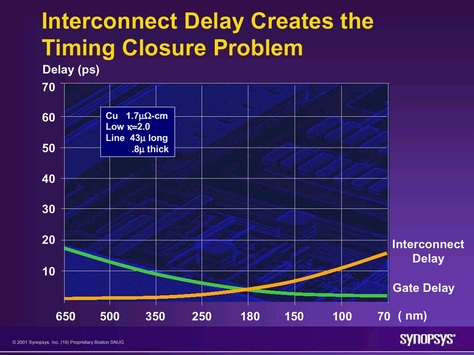
But scaling to about 0.18 micron brought us what we shall term an entanglement, which involved two inflection points. The first inflection point was the change over from transistor domination of circuit delay to interconnect domination of circuit delay.
But scaling to about 0.18 micron brought us what we shall term an entanglement, which involved two inflection points. The first inflection point was the change over from transistor domination of circuit delay to interconnect domination of circuit delay.
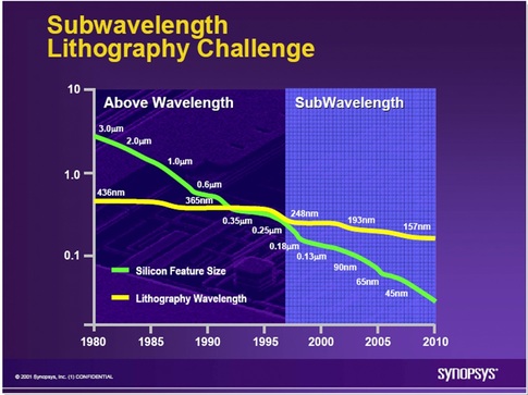
The second inflection point was sub-wavelength lithography, where the wavelength of the light used for patterning became larger than the feature being patterned.
The first inflection point drove the number of metal layers up. After years of the industry being content with two metal layers for most designs, the industry adopted three, then four, then six and eight, and now even ten or more metal layers. In addition, through hard effort and significant expenses, the industry moved from aluminum to copper and from silicon dioxide to low k dielectrics.
The second inflection point had to do with sub-wavelength lithography and brought other type of changes. First was the use of OPC and other types of reticle enhancement techniques. Then there were significant improvements of lithographic tools which involved moving from mercury lamps to excimer lasers and immersion lithography. These changes had a drastic effect on lithography equipment cost and, even more, on mask cost.
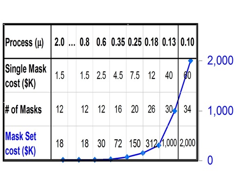
This first entanglement had a multiplicative effect on mask set cost as more metal layers required more masks, while each mask was getting more expensive. This is illustrated in the following table. (Please note that mask cost tends to get significantly reduced over time as the mask shop equipment gets depreciated)
The second inflection point had to do with sub-wavelength lithography and brought other type of changes. First was the use of OPC and other types of reticle enhancement techniques. Then there were significant improvements of lithographic tools which involved moving from mercury lamps to excimer lasers and immersion lithography. These changes had a drastic effect on lithography equipment cost and, even more, on mask cost.
This first entanglement had a multiplicative effect on mask set cost as more metal layers required more masks, while each mask was getting more expensive. This is illustrated in the following table. (Please note that mask cost tends to get significantly reduced over time as the mask shop equipment gets depreciated)
The escalating cost of a mask-set had a profound effect on IC development cost.
The escalating development cost drove the demise of the ASIC industry. For example, while at the prime time of LSI Logic there were about 50 semiconductor companies competing for the ASIC market, these days it is not clear if there even exists an ASIC market.
We now entering what seems to be a second entanglement, hence the title "entanglement squared" for this article.
On the lithography front it seems that whether we use double and triple patterning, or the long delayed EUV, the cost of lithography tools will dominate future fabs. An EUV tool is estimated to cost more than $100M.
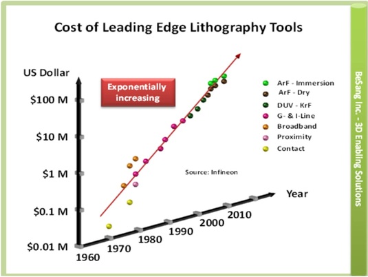
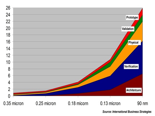
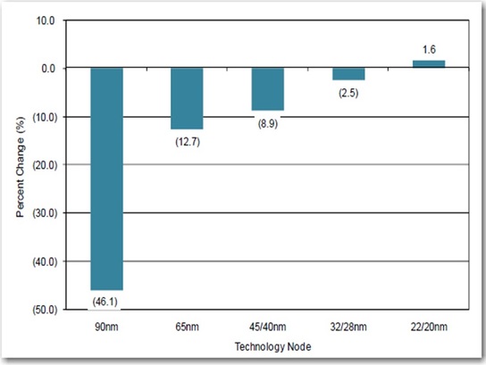
This escalating cost of lithography tools could have a profound impact on scaling. Quoting Dr. Handel Jones "For the first time since we have started following the scaling roadmap, we see an increase in cost / gate at the 22 node". His projections are shown below.
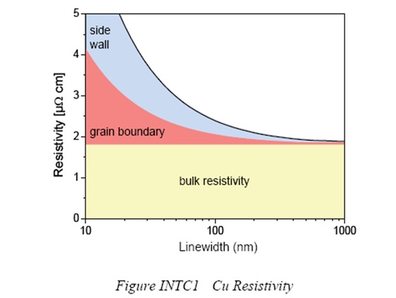
The other component of the second entanglement is interconnect scaling. Below 100nm copper resistivity escalates due to the combined effect of grain boundary scattering, side-wall scattering and diffusion barrier thickness. These escalating resistivity values will exacerbate the "tyranny of interconnects" with severe impact on chip power and performance. Clearly the chip power and speed benefits we used to get with scaling are already diminishing and this escalating resistivity is bound to have an impact.
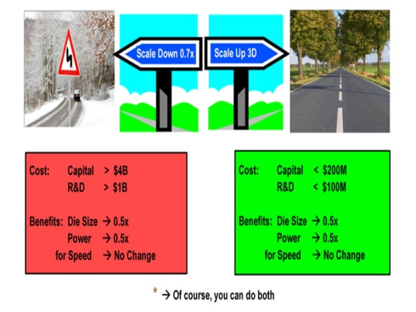
Fortunately the solution to this entanglement could come from the recent breakthrough in the feasibility of making monolithic 3D-ICs. We now have an alternative to Dennard Scaling - scaling up into the third dimension. With scaling-up, the road for continuing Moore's Law is wide open. Using the same lithography tools and the same connectivity we can double the number of transistors in a chip, with potential for chip cost reduction, performance enhancement, and power reduction, just like we used to get before.


 RSS Feed