
We have a guest contribution today from Paul Lim, MonolithIC 3D Inc.'s Principal Device Engineer. Paul is one of the best device simulation people I know, and has spent many years working on that subject. He talks about the case that device threshold voltage variations will become increasingly imposing as we scale down, especially as supply voltage is lowered.
In a previous blog post (Device Variability and Scaling), I gave an introduction to the effects of device variability on device parameters, such as threshold voltage, as we scale down. It was clear that threshold voltage variations become increasingly larger as device dimensions get smaller. At the end of the post, I promised that in a future blog I would present the case that device threshold voltage variations will become increasingly imposing as we scale down, especially as supply voltage is lowered. Well, here it is!
Threshold voltage variations are usually manageable in current digital circuits by sweeping them under the noise margin rug. However, as many of you very well know, shrinking of device dimensions leads to higher overall power consumption and necessitates lowering the supply voltage. Pretty soon, we will run out of rug space to sweep under!
As a review, let’s discuss the two big reasons why we need to scale down the supply voltage as we scale down device dimensions. The first and obvious reason is to ensure the physical integrity of the devices and avoid breakdowns. Smaller devices and thinner oxides simply can’t handle extreme electric fields.
The second reason has to do with power consumption, and there are a few aspects to this. Let us consider a single CMOS gate. For this case, if we ignore the short-circuit dissipation, the dynamic power PD is described by the familiar:
(1)
where a is the activity factor of the output node, C is the total capacitance of the output node, V is the supply voltage, and f is the operating frequency. Clearly, we can’t do very much with a, C, and f as they either stay flat or even tend to go up with nodal scaling as in the cases of C (e.g. from increasing interconnect capacitance) and f (the drive for faster chips). But not only can we do something with the supply voltage V, whatever we do with it is squared!
Static power PS can be summarized as:
Static power PS can be summarized as:

(2)
where IL is the leakage current which consists of the MOSFET sub-threshold current, gate tunneling current, and junction reverse leakage currents. All these current components increase as we scale the devices down and again, we are left with tweaking the supply voltage. So as it appears, the only way we can reduce power dissipation is by reducing the supply voltage.
There are however, also several reasons as to why we can’t keep scaling down the supply voltage. The first is that there are intrinsic material parameters that cannot be changed significantly, much less scaled, which include the bandgap energy and built-in junction potential of Silicon. Furthermore, the scaling potential of the MOSFET threshold voltage is very limited. For example, the sub-threshold leakage current for a device with a threshold voltage of 200mV is way too high and it will be hard to turn the device off. Lastly, the threshold voltage variations due to process fluctuations will force us to actually RAISE the threshold voltage to avoid having some small percentage of devices that don’t turn off.
Let us look again at the chart (Figure 1) from my previous blog post showing the trends of the supply voltage and the range of threshold voltage variations versus gate length.
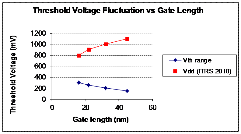
Figure 1. Range of threshold voltage variations, and supply voltage, vs. gate length, showing the increasing ratio of threshold voltage range and supply voltage as devices scale down
Figure 1 from Device Variability and Scaling
At the gate length node of 16nm, we can see that we need to raise the threshold voltage above 400mV just to accommodate the range of the threshold voltage variations, approaching the predicted 800mV supply voltage for that node. I can’t even imagine how difficult it would be beyond the 16nm node! At nodes further than 16nm, developing a manufacturing process that can handle the process variations AND maintain good yield will be prohibitively expensive. It seems that the only choices we have are either to switch to different materials (e.g. Germanium, III-V’s) or slow down scaling and go up (e.g. monolithic 3D).


 RSS Feed