
We have a guest contribution today from Paul Lim, MonolithIC 3D Inc.'s Principal Device Engineer. In this post, Paul discusses device variability and how it changes with scaling.
The end of Moore’s Law being driven by device scaling has been predicted for many years, and yet multiple innovations have fueled its continuation to the present, and are expected to do so for several more years. Despite hard physical limitations to the scaling of both conventional Silicon MOSFET devices and processes, the transition to alternate technologies has provided convenient reprieves from these harsh realities. Various sub-lithographic techniques, the use of high-k gate dielectrics, metal gates, and multiple-gate structures have each contributed tremendously to the extension of Moore’s Law. Unfortunately, the use of these same techniques has not prevented, and may have even contributed to, the increasing specter of scaling that is device manufacturing variability. I will cover a few of these issues in the following paragraphs, particularly as to their effects on the device threshold voltage.
Scaling down of feature sizes such as gate lengths and widths naturally introduce device parameter fluctuations due to dimensional effects. Simply said, the smaller the device dimensions, the greater influence edge effects and other geometric variations will have on the overall device performance. In addition, we have reached the point where the discreteness of dopants and defects in the channel region has to be considered. It must be emphasized that the effects of dopant variations are not limited to just fluctuations in doping densities, but more importantly, fluctuations in the positions and distributions of the dopants as well. The compounding effect of dopant variations on the device threshold voltage is the leading cause of device manufacturing fluctuations in current technologies. This however, will be superseded by other variation sources as we continue to scale down, and will be discussed below.
The use of high-k gate dielectrics was introduced in order to reduce gate leakage due to charge tunneling through the ever thinning silicon dioxide gate dielectrics. However, this solution presented its own problems through increased interface trap densities, which were thus subject to larger variations, resulting again in an increase in device threshold voltage variability.
The recent use of metal gates is motivated by the desire to eliminate poly-depletion in poly-silicon gates and the variations inherent in them due to their granular structure. However, the existence of metal grains in the metal gates, each with their own work-function, has led to a random distribution of the gate work-function across areas of the gate rather than a uniform deterministic value. Again this contributes to the variability of device threshold voltage.
As further scaling leads to a larger ratio of the gate area to channel region, the threshold voltage variations due to gate-related fluctuations of the work-function and interface traps will start to dominate over that of dopant fluctuations in the channel. This will be especially true in devices that employ multiple gates.
FinFET structures have been promoted as being less sensitive to parameter fluctuations because of their ability to function with lower, or intrinsic, channel doping, but this only addresses variations due to dopant fluctuations. The larger gate area to channel region ratio of FinFETs exposes them to higher gate-related fluctuations, and this ratio only gets worse with further scaling. In addition, FinFETs are inherently more sensitive to the effects of dimensional fluctuations due to process variations.
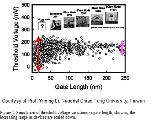
A well-known expert in studying the effects of MOSFET scaling on device parameter variations is Professor Yiming Li from National Chiao Tung University in Hsinchu, Taiwan. Figure 1 is a slide from one of his presentations that shows the increase in threshold voltage variations versus scaling of gate length, and is a great summary of the trend.
Scaling down of feature sizes such as gate lengths and widths naturally introduce device parameter fluctuations due to dimensional effects. Simply said, the smaller the device dimensions, the greater influence edge effects and other geometric variations will have on the overall device performance. In addition, we have reached the point where the discreteness of dopants and defects in the channel region has to be considered. It must be emphasized that the effects of dopant variations are not limited to just fluctuations in doping densities, but more importantly, fluctuations in the positions and distributions of the dopants as well. The compounding effect of dopant variations on the device threshold voltage is the leading cause of device manufacturing fluctuations in current technologies. This however, will be superseded by other variation sources as we continue to scale down, and will be discussed below.
The use of high-k gate dielectrics was introduced in order to reduce gate leakage due to charge tunneling through the ever thinning silicon dioxide gate dielectrics. However, this solution presented its own problems through increased interface trap densities, which were thus subject to larger variations, resulting again in an increase in device threshold voltage variability.
The recent use of metal gates is motivated by the desire to eliminate poly-depletion in poly-silicon gates and the variations inherent in them due to their granular structure. However, the existence of metal grains in the metal gates, each with their own work-function, has led to a random distribution of the gate work-function across areas of the gate rather than a uniform deterministic value. Again this contributes to the variability of device threshold voltage.
As further scaling leads to a larger ratio of the gate area to channel region, the threshold voltage variations due to gate-related fluctuations of the work-function and interface traps will start to dominate over that of dopant fluctuations in the channel. This will be especially true in devices that employ multiple gates.
FinFET structures have been promoted as being less sensitive to parameter fluctuations because of their ability to function with lower, or intrinsic, channel doping, but this only addresses variations due to dopant fluctuations. The larger gate area to channel region ratio of FinFETs exposes them to higher gate-related fluctuations, and this ratio only gets worse with further scaling. In addition, FinFETs are inherently more sensitive to the effects of dimensional fluctuations due to process variations.
A well-known expert in studying the effects of MOSFET scaling on device parameter variations is Professor Yiming Li from National Chiao Tung University in Hsinchu, Taiwan. Figure 1 is a slide from one of his presentations that shows the increase in threshold voltage variations versus scaling of gate length, and is a great summary of the trend.
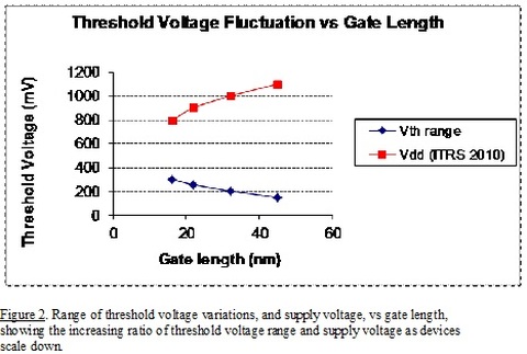
In a future blog, I will present the case that device threshold voltage variations will become increasingly imposing as we scale down, especially as supply voltage is lowered (Figure 2). Eventually, the increasing threshold voltage range and decreasing supply voltage at gate lengths of 16nm and shorter will prove untenable, and we may need to turn to other promising technologies such as 3D stacking.


 RSS Feed