
We have a guest contribution today from Brian Cronquist, MonolithIC 3D Inc.'s VP of Technology & IP. Brian discusses how can heat be removed from 3D-IC Stacks.
Thanks to everybody who came to IEDM this year, and especially to those I met and who came to paper 14.2, delivered by Hai Wei of Stanford University. You can find the meeting paper and slides here.
One of the big challenges facing 3D-IC is how to remove the heat dissipated on the upper layers to keep a high performance chip temperature within the system and reliability constraints and prevent hot spots. Most existing proposed techniques rely on arrays of TSVs and thick (xxum) silicon layer to conduct and spread the heat laterally and vertically. We propose that properly designed PDNs* (Power Delivery Networks) can significantly contribute to heat removal in both parallel (think TSV and xx um thick Si layers) and monolithic/sequential (think 100nm Si layer) 3D-ICs.
We investigated both parallel and monolithic in the paper. Here, I will, of course, focus more on the monolithic challenges and solutions, but I will make some important comparisons to parallel at the end.
Since the 130nm node, we have entered an era in our industry where we are not only using new materials, but also new device structures. I have written previously about the risk associated with this, and (hopefully…) made a case for monolithic 3D technology being the best way for the industry to move forward, still enjoying Moore’s Law type economics (i.e., lower cost) but with a much lower development risk.
Life is getting thin and narrow in our business….so, how best to take advantage of this nanometer and angstrom era and avoid the economic (think EUV at 110+M$ a pop, or double/quad patterning) and atomistic (think 7 nm) brick walls coming? Monolithic 3D stacking technology is the answer: keeping the next evolutionary step of our industry in the wafer fab, where the batch economics of the silicon wafer can be enjoyed, and avoiding the costly piece-part assembly processes of TSVs.
One of the basic tenets of monolithic 3D is the ability to have thin (preferably monocrystalline) silicon layers that enable very small vertical interconnect manufacturing, and hence a large (>1 million/cm2) layer to layer vertical interconnect density in the stack. This opens up the possibility for powerful new architectures and devices, such as Amdahl's wafer scale computer (see blog, website, technology) and cost effective MLC 3D memories.
Two implications arise from the thin (on the order of 100nm or less) silicon layer stacking. First, that fully depleted (FD) devices, and hence silicon islands floating in an insulator such as silicon dioxide, will be the norm. Second, taking full advantage of a manufacturable aspect ratio etching (5:1 to 10:1), we will end up with a large density of very small layer to layer vias (of 1-2 lambda diameter), where vertical interconnect density rivals the horizontal density of interconnect that we have enjoyed thru the many cycles of Dennard scaling. FD devices are soon to be the norm in 2DICs; for example, the thin UTBBOX of STMicro/GlobalFoundries and the narrow FinFets of Intel/TSMC (incidentally, at IEDM12, Intel was criticized for doping the fins…).
Both of these implications, FD devices in islands of Si and very dense vertical interconnect, play a significant role in how we propose to solve a major challenge in 3D stacking.
Since the stacked layers are not in direct contact with the heat sink:
How do we get the heat out of the stacked layers???
In short, the answer is to take the heat out of each silicon island with the power delivery network, move it laterally in the metal interconnect of that stack layer (just as if we had a thick silicon layer underneath), and then vertically move the heat to the heat sink with that large density of interlayer vias (which we can now make due to the thin stacked layer being very thin).
Here’s a picture of what we are doing:
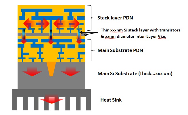
Figure 1
Sounds at least plausible, right?
Well, that’s what we set out to show, with the heavy lifting done by our friends at Stanford. Hai Wei & Tony Wu of Professor Subhasish Mitra's group, Professor Mitra, and Professor Fabian Pease, were the drivers in creating the simulation approach and engine to see if this works as we thought it might. It did, and then ended up developing a tool that may be very useful for future 3DIC design work.
Hai and Tony describe in the paper and the presentation the details of the simulation approach, engine, assumptions, and methodologies developed. Quite a nice piece of work! They have built an analysis framework that can be adapted for exploring technology-circuit-application interactions for a wide variety of 3D technologies, cooling options, and PDN designs. Types of 3DIC technologies modeled are conventional TSVs, called parallel 3D integration by many in the industry, and monolithic 3D integration, a type of sequential 3D integration. Cooling options range from conventional air cooling of the heat sink (2 W/K·cm2) to external liquid cooling (10 W/K·cm2) for high power systems. PDN designs studied ILV densities from 0 to 4 million/cm2.
That said, what are the essential takeaways?
First, the cooling benefits of PDNs are essential to achieve monolithic 3D integration. Without accounting for PDNs in the 3DIC thermal model, it will be next to impossible to achieve the desirable thermal characteristics and result of a 3D IC stack. Further, the density of ILVs is important to achieving the system thermal constraint. In the 100nm thick Si example below, the desired maximum chip temperature is 85°C or less.
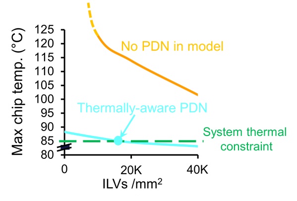
Figure 2
Second, a processor can be effectively cooled, with no hot spots, using PDNs in a monolithic 3D configuration. Hai and Tony’s thermal analyses of core-on-core and memory-on-core designs, utilizing the OpenSPARC T1 industrial multi-core design operating running an 8-threaded program that solves the Black-Scholes application (i.e., hot), showed significant improvement and no hot spots. The top silicon layer is 100nm thick and the hottest parts of the chips were operating at 138 W/cm2. Those hottest parts, the EXU units, were stacked directly on top of each other to show the worst case.
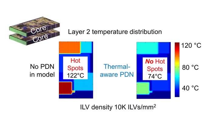
Figure 3
Combining these two seems to indicate that no PDN in the model versus designing and optimizing with thermal-aware PDNs makes the difference between being able to run the design (processor on processor in this example) at only 1/3 of the full power density or at a full power.
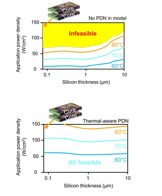
Figure 4
That’s the essential take-away for monolithic. Mimic the lateral heat conduction of thick silicon with the PDNs of the thin silicon stack layer, and then get that heat vertically to the heat sink with the dense network of vias provided by the monolithic 3D integration.
For the parallel 3D integration case, the 5um thick silicon greatly helps with the lateral heat conduction to the TSVs. With a properly designed PDN; however, there can be a significant savings in the number of TSVs (ILVs on chart below) used to vertically conduct the heat away, and thus offers a significant area savings by eliminating many of those big TSVs and Keep Out Zones (KOZs). (Note: for both the parallel and monolithic cases, Hai made the KOZ twice the ILV diameter as a conservative choice)
For the parallel 3D integration case, the 5um thick silicon greatly helps with the lateral heat conduction to the TSVs. With a properly designed PDN; however, there can be a significant savings in the number of TSVs (ILVs on chart below) used to vertically conduct the heat away, and thus offers a significant area savings by eliminating many of those big TSVs and Keep Out Zones (KOZs). (Note: for both the parallel and monolithic cases, Hai made the KOZ twice the ILV diameter as a conservative choice)
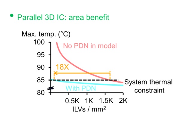
Figure 5
Moreover, by use of a properly designed PDN and an optimized density of TSVs, the maximum power density of the top layer in can be increased considerably …. from 35 to 50 W/cm2 for the parallel 3D case.
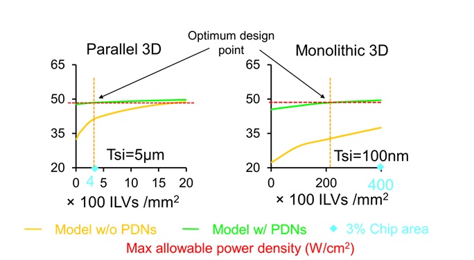
Figure 6
It is worth noting an important point from these graphs: At the optimum design point, where the density of ILVs coupled to the PDN satisfies the desired 50W/cm2 max allowed power density, the required number of TSVs to effectively conduct the heat costs about 3% of the chip area. For the monolithic case, the chip area cost is about half that.
A high density of small vias not only makes possible some powerful product architectures such as logic-cone level redundancy, but is also key to producing area efficient vertical heat conduction networks.
BC
*Patent Pending technology
A high density of small vias not only makes possible some powerful product architectures such as logic-cone level redundancy, but is also key to producing area efficient vertical heat conduction networks.
BC
*Patent Pending technology


 RSS Feed