One Learning we can take away from IEDM 2013

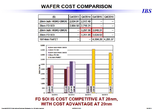
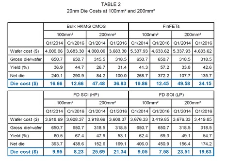
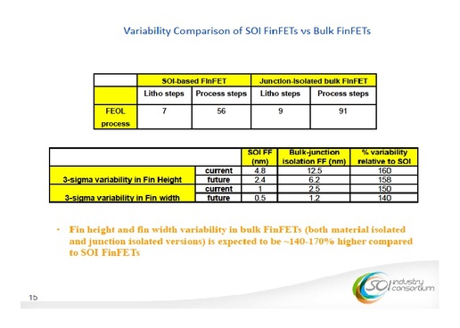
A. SOI is cheaper to fabricate than FinFet with comparable performance, and it is easier and cheaper to build FinFet on SOI which then provides better performance.
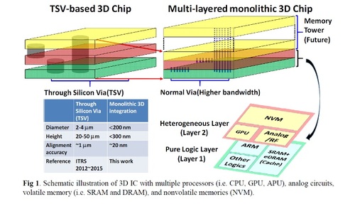
B. SOI is the natural technology for monolithic 3D IC for all overlaying transistor layers, and monolithic 3D is the most effective path to keep Moore's Law
C. SOI, or better 'XOI', is the most efficient path for most of the new concepts such as alternate materials for transistor construction and other structures like nano-wires.
Let’s now elaborate and discuss each of these points.
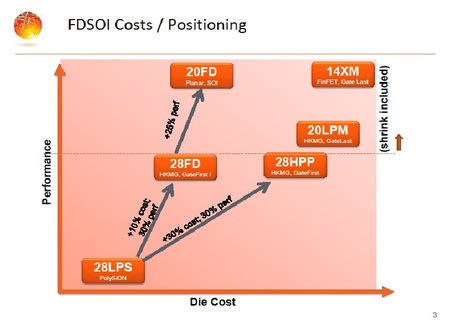
Starting with A: The following chart from Globalfoundries was presented on June 2013 at the FD-SOI Workshop, Kyoto, Japan. The chart illustrates that the best cost per transistor is the classic polysilcon gate at the 28nm node, that FD-SOI is cheaper than bulk with comparable performance at 28nm HKMG, and that FD-SOI at 20nm is cheaper than 14nm FinFet at the same performance level.
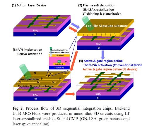
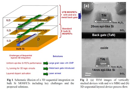
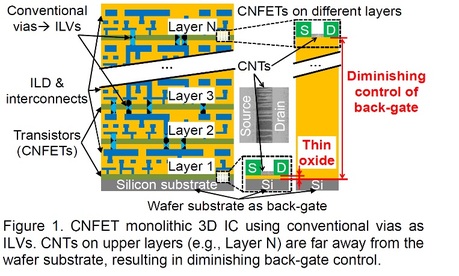
In this month’s IEDM 2013 two papers (9.3, 29.6) presented exciting demonstrations of monolithic 3D IC. It is interesting to note that Prof. Emeritus Chenming Hu of Berkeley (past TSMC CTO) who is now very famous due to his pioneering work on FinFets, is a co-author of these two pioneering works on monolithic 3D IC. The following figures illustrate the natural SOI structure of the upper transistor layers:



 RSS Feed