Sam Naffziger, an AMD Fellow, recently called for a "revolutionary improvement in on-chip interconnect to maintain the benefits of process scaling". Is the interconnect community up to the challenge?
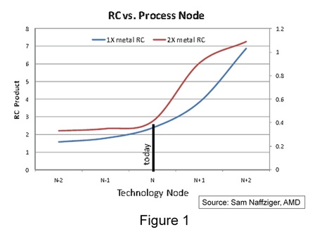
During his 2011 VLSI Symposium keynote, Sam Naffziger, an AMD Corporate Fellow showed Fig. 1 and said, "We are at the cusp of a dramatic increase in on-chip wire RC delays due to a number of factors such as small geometries resulting in increased edge effect scattering, the lack of dielectric improvement and the overhead from copper cladding layers. This trend will seriously reduce both the density and performance benefits of process scaling, so some sort of revolutionary improvement in on-chip interconnect is required."
I remember Mark Bohr, a Senior Fellow at Intel, had comments on the subject during his 2010 International Interconnect Technology Conference keynote too. He said, "There are many solutions for improving transistors, but there aren't many options for improving interconnects. We depend on you, the interconnect community, to come up with solutions."
Both Sam Naffziger and Mark Bohr were talking about logic technologies. For memory, the situation could be even worse. For a NAND flash memory chip, for instance, all bit-lines can be 10mm long and 24nm wide! The performance of the memory array is dominated by RC delay of wires.
This raises a question: What are the technological options available for improving on-chip interconnects? Let's take a look...
Silver Interconnects
Silver is the only well-known metal with higher bulk conductivity (5.6% higher) than copper. At small feature sizes though, silver loses much of this advantage, due to higher scattering effects than copper. Silver is harder to process than copper as well and is susceptible to corrosion. In terms of cost, a pound of copper costs $3.75 while a similar weight of silver costs $370. Silver is therefore not considered a viable replacement to copper: The benefits of silver over copper are negligibly small (if any) and it costs too much.
Carbon Nanotube Interconnects
Carbon nanotubes offer lower resistivity than copper. This is reflected in CNTs having mean free paths in the um range compared to 40nm for copper. They are also more resistive to electromigration and have higher thermal conductivity. However, growth of horizontally-oriented CNTs is known to be very challenging. Getting low contact resistance, high nanotube density, sub-400C CNT growth and low defect density are other unsolved issues. The research community thinks of carbon nanotube interconnects as a long term option... these are early days for the technology.
Graphene Interconnects
Graphene offers lower resistivity than copper too, with mean free paths in the 100s of nm range (compared to 40nm for copper). Other advantages could be resistance to electromigration and high thermal conductivity. However, sub-400C processing of graphene films is known to be a major challenge. Getting low contact resistance and reduced scattering at the edges are other challenges. The research community thinks of graphene interconnects as a long term option too...
3D with Through-Silicon Via Technology
We are starting to see this exciting technology move into production today. The most promising applications at the moment seem to be 3D stacked wide I/O DRAM chips, stacking DRAM atop logic and stacking heterogeneous blocks such as analog and RF atop logic. Fig. 2 shows the roadmap for TSV technology from the International Technology Roadmap for Semiconductors (ITRS). If minimum TSV dimensions are 1um or so, they are 1000x less dense than on-chip interconnects that are in the 20nm-40nm range. So, it is hard to move a big percentage of on-chip wires into the third dimension. Many therefore consider 3D-TSVs an excellent chip-to-chip interconnect solution, but not really an on-chip interconnect solution.
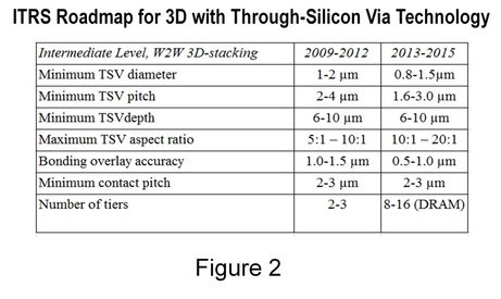
It is somewhat difficult to reduce TSV dimensions below the 500nm-1um range due to misalignment issues due to bonding and due to thickness of stacked silicon layers being in the 10um range for cost-effective manufacturing. This is reflected in the ITRS roadmap of Fig. 2 - you'll notice the minimum TSV diameter does not change much between 2009 and 2015, while on-chip interconnect dimensions reduce from 54nm to 21nm in the same time frame.
Monolithic 3D
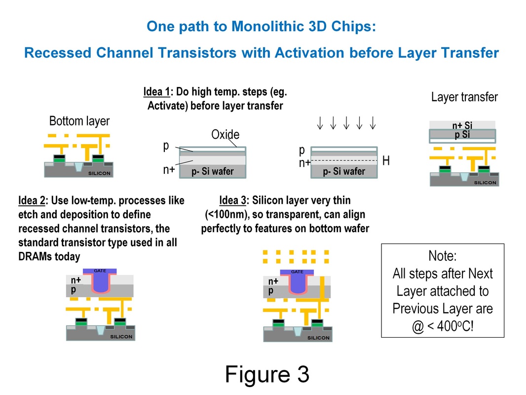
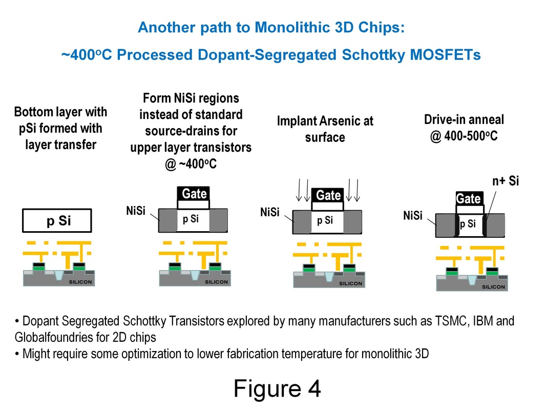
With monolithic 3D logic, the goal is to make transistors monolithically on top of interconnect levels using single crystal silicon. These c-Si layers are formed at <400C using ion-cut, the standard technique for making SOI wafers today. The biggest challenge is figuring out how to form source and drain regions of transistors at less than 400C. Multiple techniques exist for this problem, which are shown in Fig. 3, Fig. 4 and here. Since transistors are formed using thin-film processes atop copper wiring, through-silicon connections are formed with almost perfect alignment (<50nm size). Vertical connection density is comparable to horizontal connection density, allowing reduction of on-chip interconnect problems. The techniques described in Fig. 3 and Fig. 4 utilize well-known processes and materials, allowing easier adoption. Wire lengths can reduce by 30% or more by doubling the number of stacked device layers. One issue with monolithic 3D logic is that the paths shown in Fig. 3 and Fig. 4 apply transistors used today in DRAM (but not in logic) or require new transistor development. Other paths to monolithic 3D logic such as this can use any state-of-the-art gate-last transistor, but may require some sort of repeating layout to achieve the high vertical connectivity.
Monolithic 3D
With monolithic 3D logic, the goal is to make transistors monolithically on top of interconnect levels using single crystal silicon. These c-Si layers are formed at <400C using ion-cut, the standard technique for making SOI wafers today. The biggest challenge is figuring out how to form source and drain regions of transistors at less than 400C. Multiple techniques exist for this problem, which are shown in Fig. 3, Fig. 4 and here. Since transistors are formed using thin-film processes atop copper wiring, through-silicon connections are formed with almost perfect alignment (<50nm size). Vertical connection density is comparable to horizontal connection density, allowing reduction of on-chip interconnect problems. The techniques described in Fig. 3 and Fig. 4 utilize well-known processes and materials, allowing easier adoption. Wire lengths can reduce by 30% or more by doubling the number of stacked device layers. One issue with monolithic 3D logic is that the paths shown in Fig. 3 and Fig. 4 apply transistors used today in DRAM (but not in logic) or require new transistor development. Other paths to monolithic 3D logic such as this can use any state-of-the-art gate-last transistor, but may require some sort of repeating layout to achieve the high vertical connectivity.
(Click on pictures below to enlarge)
While logic makers are just starting to work on Monolithic 3D, the technology has gained significant traction in the non-volatile memory industry. Toshiba, Samsung, SanDisk and Micron have monolithic 3D on their roadmap within the next 4 years. These companies use monolithic 3D and pattern multiple memory layers with the same litho step, thereby reducing litho cost. See my old blog post on the subject here. The non-volatile memory industry scales the fastest in our industry, and hit the limits of litho faster than others. So, they started looking for alternatives to lithographic scaling first, and settled on monolithic 3D. I believe the logic industry could follow this trend soon.
In the interest of full disclosure, in case you didn't notice: I am the Chief Scientist of MonolithIC 3D Inc.
In the interest of full disclosure, in case you didn't notice: I am the Chief Scientist of MonolithIC 3D Inc.
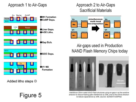
Air Gap Dielectrics
Air-gap dielectrics can provide an effective dielectric constant of 2.2-2.5, according to the ITRS. These compare with effective dielectric constants of 2.5-2.8 possible today with porous low k dielectrics. Fig. 5 shows two different air-gap schemes. Many of my friends in the logic industry are skeptical of air gaps going into production due to mechanical stability issues... I disagree with them though. Several NAND flash memory manufacturers are shipping products based on air gap technology today (see Fig. 5). These NAND flash makers did the air-gap development without too much fuss. Although the memory world is different from logic, I believe the logic industry will eventually take air gaps into production as well. The benefit of air gaps is a 10-25% reduction in capacitance, as indicated by the dielectric constant values above.
Air-gap dielectrics can provide an effective dielectric constant of 2.2-2.5, according to the ITRS. These compare with effective dielectric constants of 2.5-2.8 possible today with porous low k dielectrics. Fig. 5 shows two different air-gap schemes. Many of my friends in the logic industry are skeptical of air gaps going into production due to mechanical stability issues... I disagree with them though. Several NAND flash memory manufacturers are shipping products based on air gap technology today (see Fig. 5). These NAND flash makers did the air-gap development without too much fuss. Although the memory world is different from logic, I believe the logic industry will eventually take air gaps into production as well. The benefit of air gaps is a 10-25% reduction in capacitance, as indicated by the dielectric constant values above.
Optical Interconnects
For some of the longest interconnects on the chip, optical links might give better performance than copper, when Wavelength Division Multiplexing (WDM) is used. However, for this scenario to occur, one requires on-chip optical modulators, detectors and waveguides, which add additional masks, process steps and cost. These components currently take a lot of die area as well. Several factors are unclear, such as, for example: (1) Is having an off-chip optical source, such as a laser, viable in terms of cost and complexity? (2) Can light be bent within reasonable distances for on-chip routing? Based on analyses from Intel, IMEC and others, many experts believe the benefits of optical interconnects for on-chip applications are not worth the complexity and cost they add, at least for the next 5-10 years.
I shared some of my thoughts above. What do you think? One of our Romanian engineers, Iulia Morariu, has organized a poll where you can share your opinions. Just answer the question below and hit "vote" :-) Thank you!
- Post by Deepak Sekar


 RSS Feed