Last week, the industry was abuzz with news of Hynix's 15nm NAND flash memory technology. This important milestone brings our industry into the quad patterning era. I'll talk about quad patterning and its implications today.
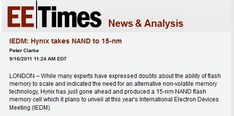
Figure 1: EETimes story on Hynix's 15nm NAND flash memory technology.
Most of us thought flash memory would never scale below 20nm. Incredibly enough, it has. Hynix has a paper at this year's International Electron Devices Meeting describing their 15nm NAND flash memory technology! An EETimes story on this topic created a buzz in our industry last week (see Figure 1). Following this, I chatted with some friends in Micron, SanDisk, Toshiba and Samsung about Hynix's announcement. Believe it or not, I heard rumors that another manufacturer has developed experimental samples of 15nm NAND flash memory too! The race to high-volume NAND flash manufacturing is indeed on...
These 15nm NAND flash products take us into the quad patterning era for lithography. The flash memory industry has used Self-Aligned Double Patterning (SADP) for the 3x and 2x nm nodes, and this technology has been extended further for 1x nm. Figure 2 gives a typical process flow for the Self-Aligned Quad Patterning (SAQP) process used for 15nm NAND flash. With deposition, etch and clean processes, features with 120nm pitch are pitch multiplied to form 15nm line-and-space (30nm pitch) patterns. One critical litho step and two non-critical litho steps are used. The process in Figure 2 is attractive because it involves fewer critical litho steps compared with other quad-patterning schemes. In addition, the critical dimension of lines to be defined is set by the thickness of the deposited spacer, which is a well known chemical vapor deposition (CVD) process and can be easily controlled to within several angstroms.
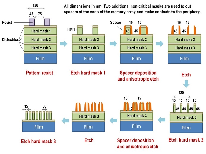
Figure 2: Self-Aligned Quad Patterning (SAQP) process used for 15nm NAND flash memory.
The striking thing about Figure 2 is the amount of work needed for a critical litho step nowadays. Obviously, such complicated processes cost a lot of money. At MonolithIC 3D Inc., we have a set of excel sheets for calculating wafer cost based on Sematech's Cost-Of-Ownership methodologies. Figure 3 shows numbers generated using these excel sheets for freshly-constructed 20,000 wspm fabs. My cost numbers approximately match estimates from TSMC and Samsung/ASML, as indicated in Figure 3. Quad patterning can cost as much as 3.7 times the cost of a single patterned lithography step! Yes, multiple-patterning is an expensive technology. Unfortunately, the industry has been forced to use it due to delays with EUV lithography.
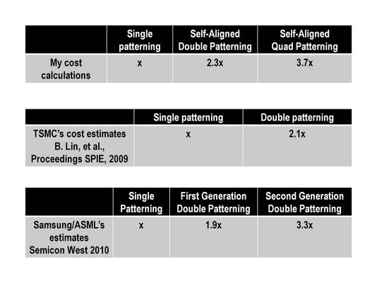
Figure 3: Cost estimates for critical litho steps using double-patterning and quad-patterning.
The estimates in Figure 3 are for freshly constructed fabs. Quite a few manufacturers upgrade their old fabs to produce a scaled technology though. Double and quad patterning are particularly amenable to reuse of cheap depreciated equipment, and this often makes them more affordable than the numbers in Figure 3 suggest. However, even with these considerations, quad-patterning is considered an extremely costly technology and companies such as TSMC, Toshiba and Mentor Graphics have talked about cost benefits of scaling ending (see [1] and [2]).
These expensive and complicated lithography technologies are giving momentum to technologies such as 450mm wafers and monolithic 3D which lower cost without complicating lithography further. Intel, Samsung, TSMC, Globalfoundries and IBM recently announced an initiative in New York to work on 450mm wafers. During negotiations for this initiative, I believe many manufacturers said litho has become expensive, and 450mm is an important way to scale the cost per transistor. Samsung, Toshiba, Hynix and Micron are aggressively investing in Monolithic 3D as a way to lower cost per bit for NAND flash as well. Roadmaps of these companies show Monolithic 3D going into volume production within 5 years. The future should be interesting...
These expensive and complicated lithography technologies are giving momentum to technologies such as 450mm wafers and monolithic 3D which lower cost without complicating lithography further. Intel, Samsung, TSMC, Globalfoundries and IBM recently announced an initiative in New York to work on 450mm wafers. During negotiations for this initiative, I believe many manufacturers said litho has become expensive, and 450mm is an important way to scale the cost per transistor. Samsung, Toshiba, Hynix and Micron are aggressively investing in Monolithic 3D as a way to lower cost per bit for NAND flash as well. Roadmaps of these companies show Monolithic 3D going into volume production within 5 years. The future should be interesting...


 RSS Feed