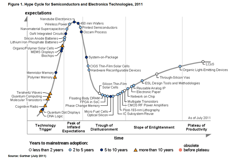
A hype cycle in Gartner's interpretation comprises five phases:
- "Technology Trigger" — The first phase of a hype cycle is the "technology trigger" or breakthrough, product launch or other event that generates significant press and interest.
- "Peak of Inflated Expectations" — In the next phase, a frenzy of publicity typically generates over-enthusiasm and unrealistic expectations.
- "Trough of Disillusionment" — Technologies enter the "trough of disillusionment" because they fail to meet expectations and quickly become unfashionable. Consequently, the press usually abandons the topic and the technology.
- "Slope of Enlightenment" — Although the press may have stopped covering the technology, some businesses continue through the "slope of enlightenment" and experiment to understand the benefits and practical application of the technology.
- "Plateau of Productivity" — A technology reaches the "plateau of productivity" as the benefits of it become widely demonstrated and accepted. The technology becomes increasingly stable and evolves in second and third generations. The final height of the plateau varies according to whether the technology is broadly applicable or benefits only a niche market.
Let's now take a look at the 2011 Semiconductor Hype Cycle, which is shown in Figure 1. I was surprised to find that Gartner's thoughts on the topic matched mine in almost all cases... I'll comment on the technologies relevant to MonolithIC 3D Inc.:
- Through-Silicon Vias (TSVs): Gartner projects this technology will become mainstream in less than 2 years. I agree. Sony, Omnivision and other image sensor manufacturers have been using TSVs for Back Side Illuminated (BSI) Sensors for some time now. Also, Xilinx announced its Virtex-7 product last week which uses multiple chips connected with TSVs and silicon interposers. TSMC is Xilinx's foundry for this technology. I am hearing rumors of Intel introducing TSVs at the 15nm node for stacking DRAM and logic... they've been buying tools from equipment makers in Silicon Valley. Yup... TSV is here!
- Networks-on-Chip (NoCs): Gartner projects mainstream adoption in 2 to 5 years. NoCs apply techniques used in communication, such as packet switching and network routers, to components of a system-on-chip. Due to the presence of shared communication links, the amount of wiring area between components of a SoC is reduced. NoC links can reduce the complexity of designing wires for predictable speed, power, noise, reliability, etc., thanks to their regular, well controlled structure.TI started using NoC technology for its OMAP products nearly 5 years back, so it is conceivable that Gartner's prediction of mainstream adoption in 2 to 5 years will work out.
- Post 193nm Lithography: Gartner foresees mainstream adoption in 2 to 5 years. EUV is the main candidate for post 193nm lithography, as you'd know. EUV has been bogged by delays for some time, and there is widespread pessimism in the industry about this technology. No wonder Gartner says it lies in the trough of disillusionment. Considering that Intel recently said EUV is late for its 10nm node in 2015/2016, I feel EUV is going to find it hard to become mainstream within 5 years.
- Phase Change Memory (PCM): According to Gartner, mainstream adoption of PCM is 2 to 5 years away, and the technology is in a trough of disillusionment now. It is easy to understand why. PCM has been dogged by manufacturing issues at Micron and Samsung, both of whom were supposed to move to high-volume production sometime back. That hasn't happened :-( Another issue is that PCM is a good candidate to replace NOR flash, but is not a good fit for replacing DRAM and NAND flash (at present). The NOR flash market has unfortunately been shrinking, leading to PCM becoming a interesting technology, but without "change-the-world market potential". Everyone's trying to 3D stack PCM, which could help it address the NAND market and increase its market potential. But the problem is not an easy one to solve. Interestingly, our company's Monolithic 3D resistive memory technology is one of the few ways to 3D stack PCM without running into temperature limitations. (In our architecture, multiple layers of single crystal silicon transistors are formed following which the PCM is deposited. So the PCM material never sees temperature higher than its 620C melting point.)
- Floating Body DRAM (FB-RAM): Mainstream adoption is 2 to 5 years away, says Gartner, and mentions that the technology is in a trough of disillusionment. Innovative Silicon, the flagship startup company in this space, went bust last year, causing pessimism about FB-RAM. In its last few years, Innovative Silicon made changes in direction, which included moving away from impact ionization (for write). Due to this, they could get higher reliability and move to sub-1V operation from 3V operation. These are important factors that could make the technology practical. However, FB-RAM still has orders of magnitude lower retention times than a capacitor-based DRAM. Innovative Silicon's investors cut funding when they found the retention problem would make it hard to compete in the stand-alone DRAM market, even though the embedded DRAM market was viable. Micron bought Innovative Silicon's IP and is working on the technology now, I hear. Check out our company's Monolithic 3D DRAM technology, if you get a chance. We bring 3D stacking, shared litho steps, novel refresh schemes and various other tricks to FB-RAM technology, which will hopefully make it viable.
- Memristor Memory: Memristors, also called RRAM, are 5-10 years away, according to Gartner. I've worked on RRAM for some time now, and have given talks about the topic in various forums. I must say that my assessment matches with Gartner's. At MonolithIC 3D Inc., we've developed a 3D resistive memory architecture that is quite interesting... read my blog post about the architecture here. There are still many unsolved challenges with RRAM. Reset current needs to be lowered without compromising retention, forming voltages are high, there aren't enough array demonstrations, etc. Hopefully, these challenges will be resolved with time.
- Post by Deepak Sekar


 RSS Feed