Consider the following points in bold:
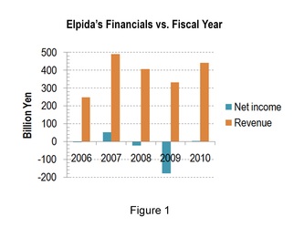
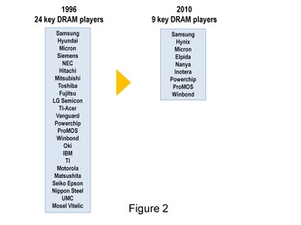
- We've seen a carnage in the DRAM industry over the past two decades: Fig. 1 shows the financials of a top-tier DRAM vendor, Elpida, over the past 5 years. You'll see it's a hard business to be in... there's not much profit to be made. The story is similar for most other DRAM vendors in the near past - they've lost more money than they've made :-( This has resulted in the trend shown in Fig. 2. A big percentage of DRAM vendors have exited the market.
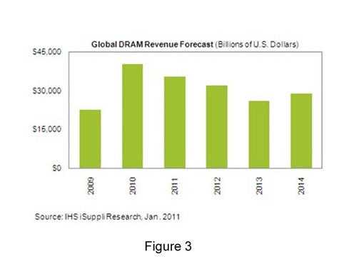
- Market projections for the future don't look very rosy either: According to iSuppli, the DRAM market is projected to shrink from ~$40B in 2010 to ~$28B in 2014. While the market size is huge, there's an average decline of 9% every year :-( It's going to be a very choppy ride for DRAM vendors who choose to stay in a shrinking commodity market!
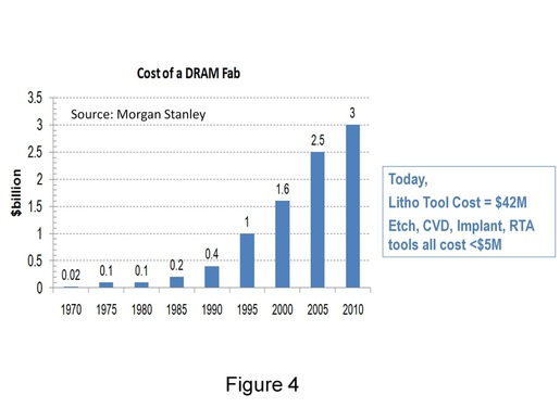
- Fabs for smaller feature sizes will cost an arm and a leg: Moving to smaller feature sizes has historically helped vendors bring their costs down and tackle the price declines inherent in the DRAM market. However, the prices for fabs have risen exponentially over the past few years as Fig. 4 shows, and a DRAM fab now costs a whopping $3 billion! This makes it difficult for most DRAM vendors to afford scaled-down fabs, since they haven't been very profitable in the near past (as Fig. 1 shows). Also note that these large fab investments are partly the reason for the low net income numbers shown in Fig. 1. The culprit for this exponential increase in fab prices is indicated in Fig. 4. It's mainly the litho tools - they cost a lot more than any other tool in the fab. If we scale down to smaller feature sizes, the litho is projected to get much more expensive, making future scaling down even more difficult. An EUV tool is projected to cost $100M!
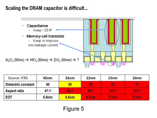
- The DRAM capacitor gets very challenging at smaller feature sizes: We talked about difficult business conditions in Fig. 1-Fig. 4. But wait, there are huge technology challenges with scaling-down too. If you look at projections from the Intl. Technology Roadmap for Semiconductors (ITRS) in Fig. 5, stacked capacitors require aspect ratios close to 200:1 in future technology generations. Just to put this in perspective, 10:1 aspect ratios are considered tough in many parts of the industry today. Note how the ITRS has shaded aspect ratios above 50:1 in red, which indicates "no known solution". Furthermore, well-known high-k materials such as hafnium oxide, zirconium oxide and aluminum oxide have already been used in past generations, and future generations will require exotic new high-k dielectrics with dielectric constants around 70, according to the ITRS.
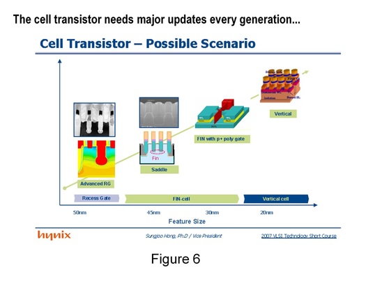
- The cell transistor needs a lot of work for smaller feature sizes: The DRAM industry moved from planar cell transistors to recessed channel array transistors (RCATs) around the 80nm node, and then moved to spherical RCATs (S-RCATs) around the 70-60nm nodes. Fig. 6 shows Hynix's roadmap for cell transistors... it requires major changes in the transistor for every scaled technology generation! It is a lot of work!!
We've seen that the DRAM industry is facing huge and potentially disruptive challenges right now. A lot of it has to do with scaling-down and the huge investments (fab costs) it needs, and also the continuous overhaul of the DRAM capacitor and the cell transistor it requires. Is there a way out of this mess?
Yes, there could be.
If you're interested to know more about this solution, come hear my talk on Wednesday at the American Vacuum Society Workshop on 3D Technology. It's going to be in San Jose, and entry is free :-) For more details of this workshop, check out this link.
PS: I hope this blog-piece has piqued your interest in my talk :-)



 RSS Feed