
We have a guest contribution today from Zvi Or-Bach, the President and CEO of Monolithic 3D Inc. Zvi argues that the EDA vendors need to form relationships with their customers that allows the tool companies to share the risks and rewards that come with striving for improved yields.
For the past few decades, I have heard EDA industry leaders complaining about being the enablers of the semiconductor industry’s production while being poorly compensated for the value created by their tools. As I recall, it was Joe Costello, Cadence CEO at the time, who gave up on the possibility of being able to derive EDA compensation from device volume production. Instead, he initiated the change of the EDA business model from the perpetual license to a time-limited three-year license. As for myself, I never understood the point. Think about it—Boeing is not compensated for the airlines’ revenues enabled by its planes.
But living in the Semi world is all about change. And, for every few technology nodes, the incremental change turns into fundamental change. We are facing one now in the role of EDA vendors for semi volume yields.
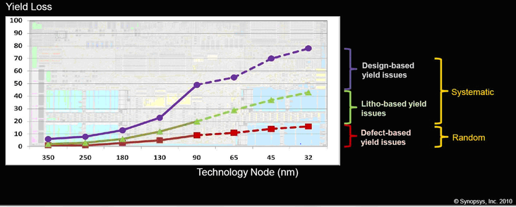
The following chart, courtesy of Synopsys, illustrates the change from the days when device yields were mostly a function of the fab defect density to the current situation, and shows us the next technology nodes, when yield will be dominated by “design-based yield issues.”
The following chart, courtesy of Synopsys, illustrates the change from the days when device yields were mostly a function of the fab defect density to the current situation, and shows us the next technology nodes, when yield will be dominated by “design-based yield issues.”
To understand these issues better we just need to look into the trend related to device modeling and manufacturing rules.
Current thoughts on custom IC design.
In James Hogan’s viewpoint article, titled “Current thoughts on custom IC design” (EE Times of 5/18/2010), he wrote: “As custom designers shift to today’s 45nm, 32nm and 28nm technology nodes, they encounter exponentially worse variation issues, … In the past, there were only 5-20 PVT corners to analyze, but for custom designers to properly bound variation in modern technologies, they need to investigate more variables and more values per variable, leading to thousands of corners.” Those who are familiar with circuit design (polygon style) have seen the number of design rules increase from less than 200 rules at 0.18u and above to over a thousand at 65nm. As reported by R Colin Johnson (EE Times, 3/31/2010) IBM warns of design rule explosion beyond 22-nm: "Simple technology abstractions that have worked for many generations like rectangular shapes, Boolean design rules, and constant parameters will not suffice to enable us to push designs to the ultimate levels of performance."
The historical EDA acquisition process was all about benchmarking EDA tools against run time and end device performance (speed, area, power). Those could be checked up-front and supported the existing business model. But up-front checks will not be sufficient for future SoC designs. In fact, ultimate device yield can be measured only at the far end of the process and replacing the EDA tools then is akin to closing the barn door after the horse has bolted. Vertically integrated companies, like Intel, clearly have an advantage in assuring that all necessary steps are taken by their EDA department to get the best yield possible. But fabless SoC vendors, who buy standard off the shelf EDA tools, are left in the position of ‘buy and pray’.
As design-based yield issues become so significant – like ~50% of yield loss, it seems that some form of partnership between SoC vendors and their EDA tools suppliers needs to be established, wherein the EDA vendors have an incentive to do whatever is necessary not just to win the design but also to win the down-the-road production yield.
And yes, there is one other alternative – the one we at MonolithIC 3D believe in. Now that monolithic 3D is practical, there is an alternative to the classical scaling (i.e., scaling down). Device complexity can be doubled with the many other benefits in power and performance by “scaling up” instead into the third dimension – building 3D IC. Scaling up would imply using the same tuned and yielding process node again and again, reversing many of the trends presented above.


 RSS Feed