
We have a guest contribution from Zvi Or-Bach, the President and CEO of MonolithIC 3D Inc. Mr. Or-Bach discusses about the new trend in semiconductors for equipment spending.
A recent Semi™ report titled SEMI Reports Shift in Semiconductor Capacity and Equipment Spending Trends reveals an important new trend in semiconductors: "spending trends for the semiconductor industry have changed. Before 2009, capacity expansion corresponded closely to fab equipment spending. Now more money is spent on upgrading existing facilities, while new capacity additions are occurring at a lower pace, to levels previously seen only during an economic or industry-wide slowdown".
Looking at the semi-equipment booking should be the first step in any attempt to assess future semiconductor trends. While talking is easy, spending billions of dollars is not. Vendors look deeply into their new design bookings and their future production needs before committing new dollars to long lead purchases for their manufacturing future needs. In the past decade it was relatively simple, as soon as a new process node reached production maturity vendors would place new equipment orders knowing that soon enough all new designs and their volume will shift to the new process node. But the Semi™ report seems to tell us that we are facing a new reality in the semiconductor industry – a Paradigm Shift.
A while ago VLSI Research Inc. released the following chart with the question: Is Moore’s Law slowing down?

Figure 1
The chart above indicates a coming change in the industry dynamic, and 2013 might be the year that this turns out to be a Paradigm Shift.
Just few weeks ago at the SEMI ISS conference, Handel Jones of IBS presented many very illuminating charts and forecasts. The following chart might be the most important of them and it is the revised calculation of per gate cost with scaling.
Just few weeks ago at the SEMI ISS conference, Handel Jones of IBS presented many very illuminating charts and forecasts. The following chart might be the most important of them and it is the revised calculation of per gate cost with scaling.
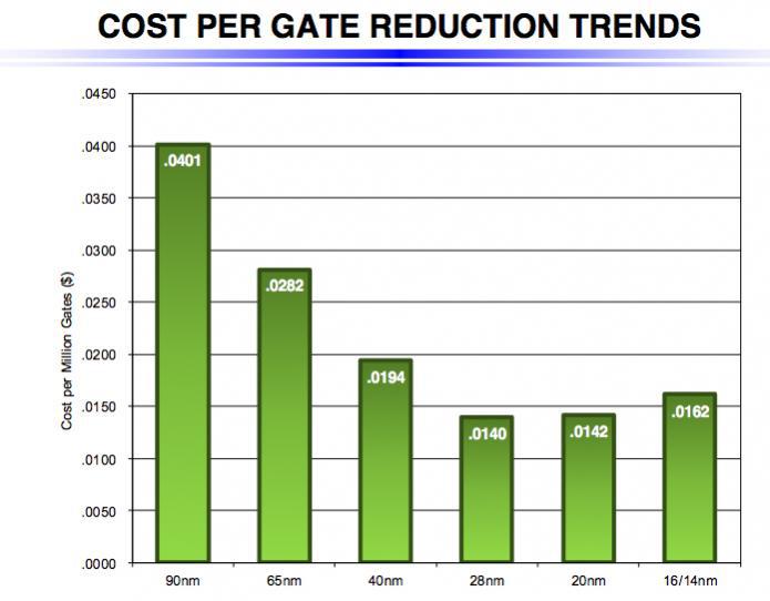
Figure 2
Clearly the chart reveals an unmistakable Paradigm Shift as 28nm is the last node for which dimensional scaling provides a per gate cost reduction. It makes prefect sense for the vendors and their leading edge customers to respond accordingly. Hence it easy to understand why more equipment is being bought to support 28nm and older nodes.
The following table, also from Jones, illustrates this new reality.
The following table, also from Jones, illustrates this new reality.
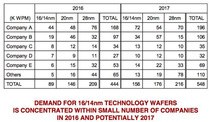
Figure 3
In the equipment business, more than 50% of demand comes from the memory segment where the dollars per sold wafer are much lower than in logic. It seems that the shift there has already taken place. Quoting Randhir Thakur, Executive Vice President, General Manager, Silicon Systems Group, Applied Materials, Inc -as was recently published in The shift to materials-enabled 3D: " our foundry/logic and memory customers that manufacture semiconductors are migrating from lithography-enabled 2D transistors and 2D NAND to materials-enabled 3D transistors and 3D NAND"..."Another exciting inflection in 2014 is our memory customers’ transition from planar two-dimensional NAND to vertical three-dimensional NAND. 3D technology holds the promise of terabit-era capacity and lower costs by enabling denser device packing, the most fundamental requirement for memory". Which fits nicely with the following illustration made by Samsung as part of their 3D-NAND marketing campaign.
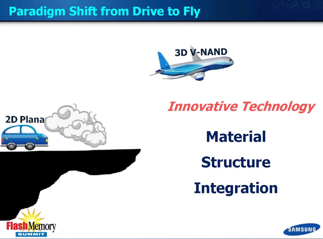
Figure 4
As for the logic segment, the 3D option is yet to happen. But as we wrote in respect to 2013 IEDM - More Momentum Builds for Monolithic 3D ICs. The following chart from CEA Leti illustrates the interest for monolithic 3D:
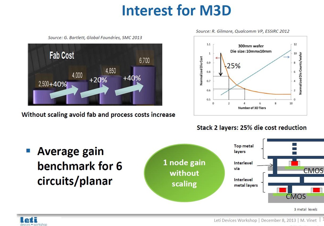
Figure 5
It should be noted that monolithic 3D technology for logic is far behind in comparison to memory. Given that the current issues with dimensional scaling are clearly only going to get worse, we should hope that an acceleration of the effort for logic monolithic 3D will take place soon. In his invited paper at IEDM 2013, Geoffrey Yeap, VP of Technology at Qualcomm, articulates why monolithic 3D is the most effective path for the semiconductor future: "Monolithic 3D (M3D) is an emerging integration technology poised to reduce the gap significantly between transistors and interconnect delays to extend the semiconductor roadmap way beyond the 2D scaling trajectory predicted by Moore’s Law." As illustrated by his Fig. 17 below.

Figure 6
So, in conclusion, our industry is now going thru a paradigm shift. Monolithic 3D is shaping up as one of the technologies that would revive and sustain the historically enjoyed growth and improvements well into the future. The 2014 S3S conference scheduled for October 6-9, 2014 at the Westin San Francisco Airport will provide both educational opportunities and cutting edge research in monolithic 3D and other supporting domains. Please mark your calendar for this opportunity to contribute and learn about the new and exciting monolithic 3D technology.


 RSS Feed