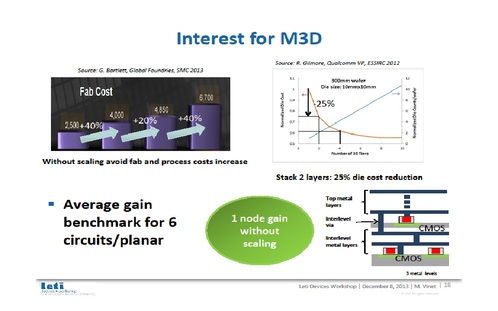
Clearly dimensional scaling is not providing transistor cost reduction beyond 28 nm node, and the large fabless companies--Qualcomm, Broadcom, Nvidia, and AMD—recently reported this fact again. The industry is trying to accommodate this new reality, while still rushing to develop and adopt more advanced nodes at escalating costs and complexity. Consequently, the door has started to open for other kinds of technology that might help to maintain the industry’s overall momentum, and monolithic 3D ICs seem well positioned to do so. 3D NAND is the first segment of the industry to adopt this new path for scaling, as was reported in early August this year: Monolithic 3D is now in production: Samsung starts mass producing first 3D vertical NAND flash. A few months afterward we learned that Besang signed a license agreement with Hynix for their monolithic 3D technology, which might help Hynix to offer more competitive 3D DRAM. Then we learned that Singapore-MIT Alliance for Research Technology ordered EV Group automated production bonding system, for integrating silicon CMOS and compound semiconductor materials to enable new integrated circuits for wireless devices and power electronics. And just last week CEA Leti announced an agreement with Qualcomm to Evaluate Leti’s Non-TSV 3D Process.
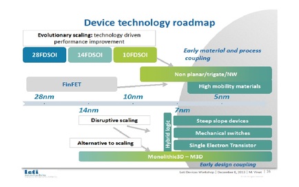
Thus it fitted very well for Leti to include in their presentation event done in conjunction with this year’s IEDM 2013, slides promoting monolithic 3D as an alternative to dimensional scaling as is presented in the following slide:


 RSS Feed