
We have a guest contribution today from Brian Cronquist, MonolithIC 3D Inc.'s VP of Technology. Brian shares his perspective on Low Temperature Wafer Direct Bonding, where an important concern is the strength of the wafer to wafer oxide to oxide bond.
Sometimes we get questions about a particular aspect of the monolithic 3DIC flow. In this blog I would like to talk about Low Temperature Wafer Direct Bonding, where an important concern is the strength of the wafer to wafer oxide to oxide bond. Can it survive the subsequent transistor formation or wafer thinning processing, whether that processing entails the shear forces of a CMP, the thermal gradients of a low temperature deposition, or the stress release of a plasma or wet etch?
Direct wafer bonding is both desirable and required for low cost high yield monolithic 3D integration. “Direct” meaning that an extra layer, an intermediate layer, such as an adhesive, is not used. The bonding between the surfaces only involves the chemical bonds between the two surfaces. The simplest case for a conventional wafer fab, which has the highest probability of achieving high yield & low cost direct bonding, is oxide to oxide bonding. Oxide to oxide wafer bonding has the added advantage that a through layer via connection may not need an isolation liner, and is part of a process integration strategy that delivers a Thorough Layer Via (TLV) with processing ease and characteristics similar to a conventional BEOL metal to metal via.
Another enabler for monolithic 3D integration is a direct bonding process that has thermal exposures to the underlying layer or layers that does not exceed 400°C. This allows the use of conventional metallization and low-k dielectrics such as copper & carbon containing low-k oxides BEOL, rather than difficult to manufacture high temperature metals such as tungsten. Two additional advantages of low temperature bonding are avoiding any wafer deformation due to thermal expansion effects (greatly helps across the wafer alignment precision), and minimizing the thermal effects on the lower layer transistor hi-k metal gate stacks and junctions.
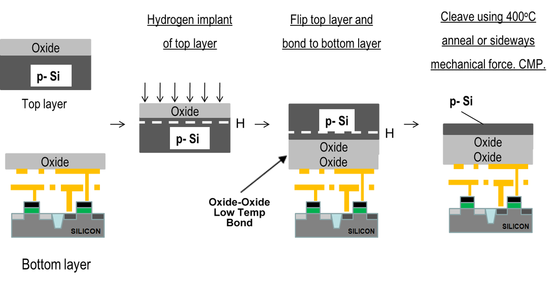
Figure 1 Low Temperature Wafer Direct Bonding
The generally accepted strength threshold metric of a wafer to wafer bond that would enable thinning, such as CMP, and other processing (<400°C), is between 1.0 and 1.2 J/m2. Di Cioccio talks about 1.14 J/m2 bond strength as sustaining processing such as silicon thinning (backgrind and CMP). Dragoi shows that surface energies above 1.2 J/m2 allow bonded pairs to survive even harsh processes as grinding or lapping. Radu found that a bonding strength of more than 1 J/m2 has been sufficient to sustain post-processes such as silicon back thinning using coarse and fine grinding.
Many investigators, groups and companies have developed pre-bonding surface conditioning and post-bonding thermal treatments to control and optimize the bonding strength within the constrained thermal budget window (<400°C) and have achieved excellent bond strength’s greater than 1 J/m2. A sampling of the literature follows:
DiCioccio et al. at ICICDT 2010 [CEA-LETI-Minatec, Grenoble, USA] showed acceptable bonding strengths from bonded wafers with 5um copper pads that cover 20% of the area, the remainder is oxide to oxide, after a 2 hour 200°C or 400°C post bond anneal. The surfaces were carefully prepared with CMP.
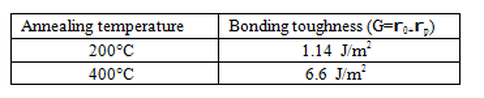
Table 1 : Bonding toughness (G=r0+r) of the bonding pair as a function of the post bonding annealing temperature. The annealing step was 2h long.
Radu et al. at the 2010 3DIC conference [Soitec Bernin, CEA-LETI-Minatec, Soitec USA], showed bonding energy data obtained from 200mm wafer bonding of Cu/Cu full sheet, SiO2/SiO2 full sheet, Cu/SiO2 full sheet, and pattered 5um Cu pads at 20% density. Oxide to oxide bonding at 200°C produces over 1 J/m2 bonding energy. The surfaces were carefully prepared with CMP.
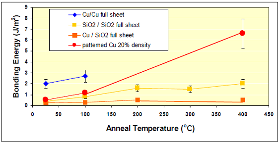
Figure 2 Bonding energy evolution with temperature of different type of interfaces (Cu-Cu, Cu-Ox and Ox-Ox)
Gaudin et al. at 3DIC 2010 [Soitec Grenoble, Soitec USA, IBM Albany, IBM East Fishkill] utilized 300mm wafers with a backend CMOS process and deposited oxide layer acting as the bonding layer. Bonding surfaces were prepared with an optimized CMP process and post-bond annealing, thinning and grinding were successfully performed. Gaudin studied one TEOS-based oxide and two different condition sets for silane-based PECVD oxide. Silane condition B was certainly superior and exceeded the 1 J/m2 metric at both 200°C and 400°C.
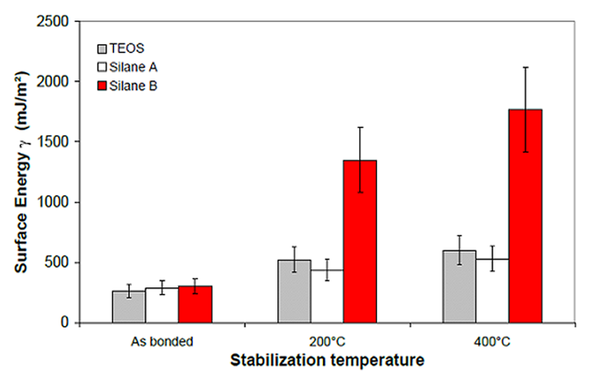
Figure 3 Surface energy (γ) evolution with temperature of oxide bonding stacks using 3 different deposited oxides
Gaudin further influenced the bonding quality by conditioning the surface with wet chemical processing (Process I) and dry plasma processing (Process II).
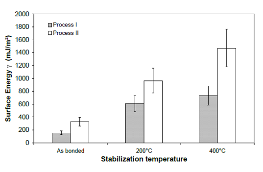
Figure 4 Surface energy (γ) evolution with temperature for 2 surface preparation process options on a TEOS based oxide
Dragoi et al. at SPIE 2007 [EV Group] showed blank wafer data where a PECVD oxide was deposited, outgassed in a vacuum anneal at 300-400°C 1-3 hr anneal, CMP polished, nitrogen plasma activated, megasonic cleaned, vacuum bonded with 5kN force, then annealed for 1 hour at 300°C.
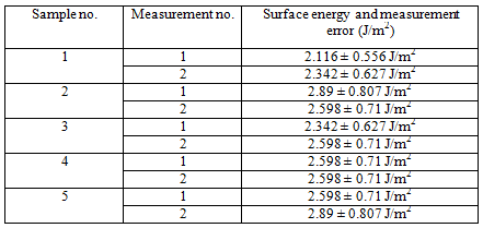
Tabel 2 Bond strength measured for sample 1
Dragoi successfully applied the process on 200mm Si on CMOS bond pairs.
Sadaka et al. in electroiq.com (2010) [Soitec USA, CEA-DRT-LETI] showed 3 different processes (CMP/surface conditioning/planarization/cleaning). With 200°C, 350°C or 400°C post bond anneals, the target of 1 J/m2 was achieved.
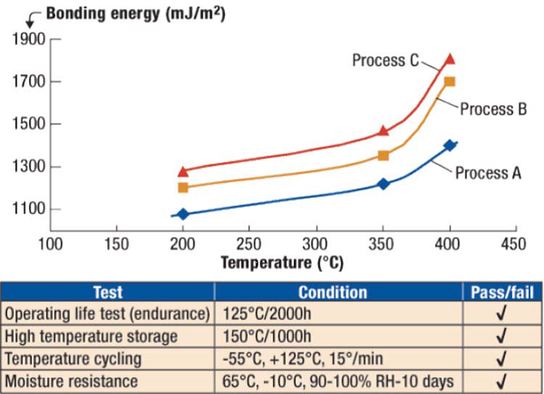
Figure 5
Ziptronix talks about their DBI (Direct Bond Interconnect) technology as utilizing RIE surface cleans & porosity enhancement, NH4OH surface treatments, CMP to 0.5nm RMS, and obtaining bond energies >1 J/m2 at room temperature.
Henttinen et al. in Applied Physics Letters April 2000 [VTT Electronics, Finland; UC San Diego] demonstrated oxide to oxide bonding of silicon wafers with various plasma or RCA clean pretreatments, and post-bond thermal anneals.
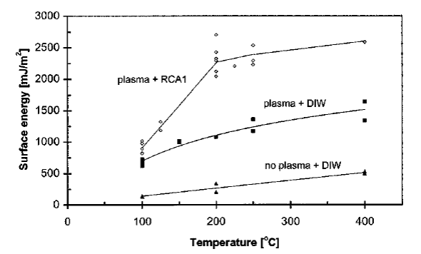
Figure 6 Bond strength of the bonded interface as a function of bond annealing temperature. The annealing time varied between 30 min and 24h.
SiGen Corporation reported in 1999 and 2000 the use of a plasma activated pre-bond step to achieve >1 J/m2 bonding strength.
In summary, a variety of investigators have shown processes capable of providing excellent wafer to wafer bond strengths.
References:
DICIOCCIO, L., et al., "Direct bonding for wafer level 3D integration", ICICDT 2010, pp. 110-113.
DRAGOI, et al., “Plasma-activated wafer bonding: the new low-temperature tool for MEMS fabrication”, Proc. SPIE, Vol. 6589, 65890T (2007).
RADU, I., et al., "Recent Developments of Cu-Cu non-thermo compression bonding for wafer-to-wafer 3D stacking", IEEE 3D Systems Integration Conference (3DIC), 16-18 Nov. 2010.
GAUDIN, G., et al., "Low temperature direct wafer to wafer bonding for 3D integration", 3D Systems Integration Conference (3DIC), IEEE, 2010, Munich, 16-18 Nov. 2010, pp. 1-4.
SADAKA, M., et al., "Building Blocks for wafer level 3D integration", www.electroiq.com, August 18, 2010.
www.ziptronix.com, DBI fact sheet
HENTTINEN, K. et al., "Mechanically Induced Si Layer Transfer in Hydrogen-Implanted Si Wafers," Applied Physics Letters, April 24, 2000, p. 2370-2372, Vol. 76, No. 17.
I.J. MALIK, et al., “The Genesis Process: A general layer transfer method for electronic applications,” Spring 10999 MRS Symp. Tech. Proc., 1999
F.J. HENLEY, et al., European Semiconductor, 25, Feb. 2000.


 RSS Feed