For the past 40 years, semiconductor technologists relied on improvements in lithography to "cram more components onto integrated circuits". Toshiba, Samsung and other non-volatile memory companies are betting the future will be different. Let's look at the fascinating idea they're pursuing...
I'm going to begin by making three provocative statements:
- Lithography is expensive.
- Lithography doesn't give you as much bang for the buck as it used to.
- Lithography is never on time.

Let's move on to the second statement. In past years, transistors improved as they scaled down. Not so anymore... With smaller feature sizes, flash memory cells, for example, get much worse - you have more variability and far wider threshold voltage distributions (makes it difficult to store MLC), endurance gets worse (many manufacturers can do just 500 cycles today) and you need to move to extremely sophisticated error control coding. Device physicists out there may find the next sentence shocking. Many latest generation flash memory cells have sub-threshold slopes greater than 450mV/decade! Scaling has indeed wrecked havoc on the quality of flash memory cells.
The third statement, that litho is never on time, is easy to justify. Here are a few quotes made by industry folks to EETimes over the years :-)
(2002) "EUV to be in production in 2007"
(2003) "EUV to be leading candidate for the 32nm node in 2009"
(2004) "EUV to be pushed out to 2013"
(2010) "EUV late for 10nm node milestone in 2015"
With EUV getting delayed so much, the industry has moved to costly double patterning techniques and now we have quad patterning on the horizon. This is particularly problematic for technologies such as NAND flash memory, where people need to move to the next generation once a year (compared to once every 2-3 years for logic and DRAM).
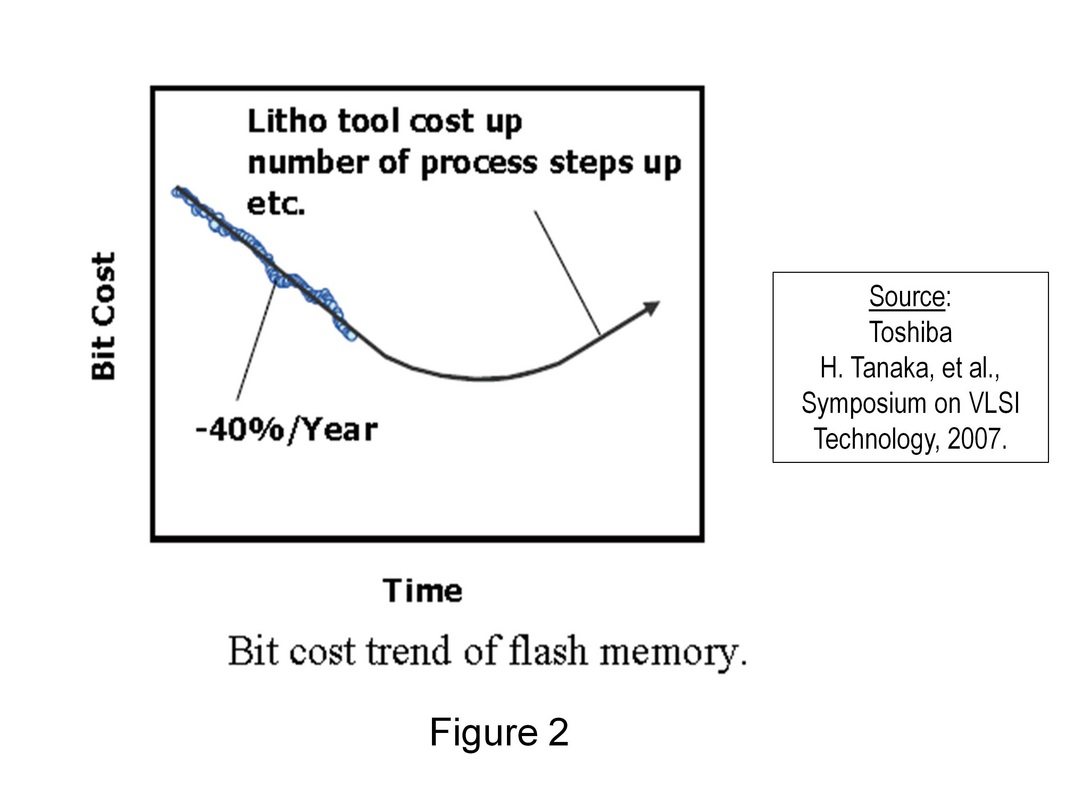
The net effect of all these trends is the plot shown in Fig. 2 from Toshiba. They say litho costs are becoming so high that moving to smaller feature sizes may not always lead to cheaper NAND flash memory products. While one could argue about the Toshiba plot in Fig. 2, it is clear that any way to break our dependency on lithographic scaling will be great.
How can we break our dependence on lithographic scaling?
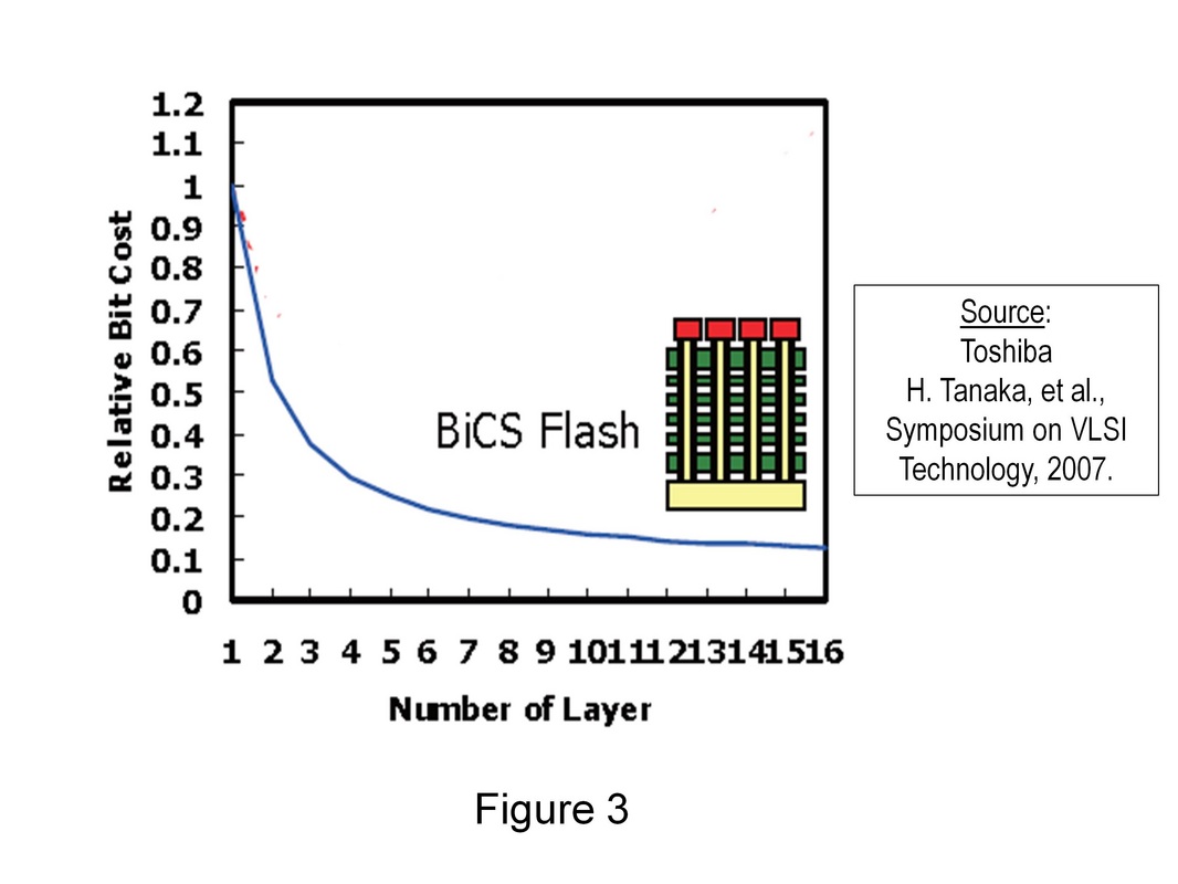
Almost all non-volatile memory firms are exploring different versions of the following idea: Build monolithic 3D chips where multiple levels of memory share the same lithography steps. If you have 8 memory cell layers, for instance, and you use one set of litho steps for defining all these 8 layers, you get a 8x increase in memory density compared to a single memory layer 2D chip, but without increasing the dreaded litho cost. This results in a net reduction in bit cost, as shown in Fig. 3.
The third statement, that litho is never on time, is easy to justify. Here are a few quotes made by industry folks to EETimes over the years :-)
(2002) "EUV to be in production in 2007"
(2003) "EUV to be leading candidate for the 32nm node in 2009"
(2004) "EUV to be pushed out to 2013"
(2010) "EUV late for 10nm node milestone in 2015"
With EUV getting delayed so much, the industry has moved to costly double patterning techniques and now we have quad patterning on the horizon. This is particularly problematic for technologies such as NAND flash memory, where people need to move to the next generation once a year (compared to once every 2-3 years for logic and DRAM).
The net effect of all these trends is the plot shown in Fig. 2 from Toshiba. They say litho costs are becoming so high that moving to smaller feature sizes may not always lead to cheaper NAND flash memory products. While one could argue about the Toshiba plot in Fig. 2, it is clear that any way to break our dependency on lithographic scaling will be great.
How can we break our dependence on lithographic scaling?
Almost all non-volatile memory firms are exploring different versions of the following idea: Build monolithic 3D chips where multiple levels of memory share the same lithography steps. If you have 8 memory cell layers, for instance, and you use one set of litho steps for defining all these 8 layers, you get a 8x increase in memory density compared to a single memory layer 2D chip, but without increasing the dreaded litho cost. This results in a net reduction in bit cost, as shown in Fig. 3.
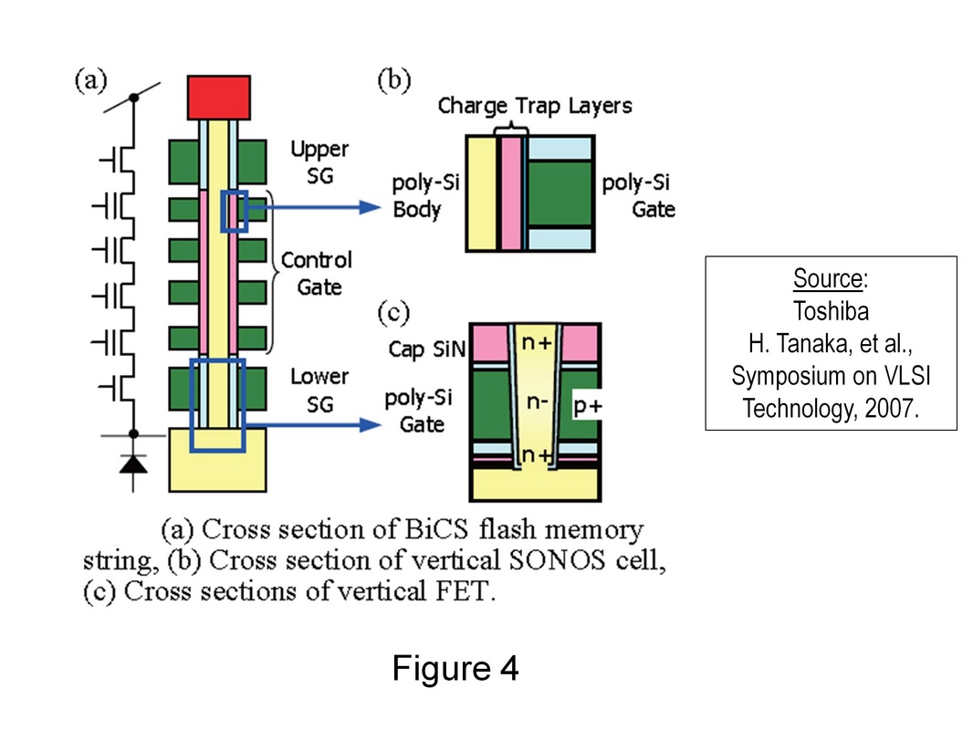
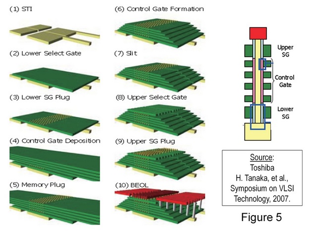
Let's explain the concept further using Toshiba's figures, reproduced in Fig. 4 and Fig. 5. Toshiba was a pioneer of this "monolithic 3D with shared litho steps" concept and presented their Bit Cost Scalable (BiCS) technology at the Symposium on VLSI Technology in 2007. Fig. 4 shows the basic memory structure. You have a NAND string built vertically where each NAND transistor is a SONOS charge-trap memory cell. The channel of the device is constructed out of poly silicon. Fig. 5 shows the process steps required for constructing the 3D memory array. You'll notice that litho steps required, such as Step 5 for etching and filling to form the polysilicon channel and Step 10 for the BEOL are shared among all memory layers. Litho needed for Step 6 is shared among all memory layers using a neat trick described in the Toshiba paper (I'm not going to describe it here since this blog post is getting too long!). The take-home point is that we form multiple levels of memory without increasing the litho cost significantly.
How can this idea break our dependency on lithographic scaling? Well, if you share litho steps among all layers of memory, you can reduce bit cost by having more memory layers. For example, if you have 4 layers of memory for a certain generation, you could have 8 layers of memory for the next generation, thereby keeping litho cost constant and reducing bit cost. Of course, the aspect ratios of vias to be etched and filled increases. For the 4 layer memory, you might have an aspect ratio of 10:1 while for the 8 layer memory, you'd have an aspect ratio of 20:1. And for the next node, you'd have an aspect ratio of 40:1. Essentially, you need to figure out techniques to etch and deposit vias of higher aspect ratio every generation. DRAM capacitors made today have aspect ratios of 70:1, so it is indeed possible that we could get several generations of scaling using technologies such as BiCS.
Outlook
Should we then forget about improving our litho tools and concentrate instead on these new monolithic 3D architectures? The answer is no. BiCS has several challenges: it uses polysilicon channels for it's NAND strings, it uses charge-trap devices that are known to be hard to take to production, aspect ratios required for cost effective products can go to 40:1 which are very high, just to list a few. But then, the whole NAND flash memory industry, which includes Samsung, Macronix, Hynix and Intel/Micron, has started pursuing this technology... this industry momentum has produced several enhancements to the basic idea proposed by Toshiba. The technology appears more and more practical with every passing year.
What connection does MonolithIC 3D Inc. have with all this?
Like I mentioned above, one of the key challenges with the approaches pursued by Toshiba, Samsung and others is the use of polysilicon channels for transistors. This can cause variability and wide threshold voltage distributions (difficult for MLC), low mobility (low read current) and bad yield. We at MonolithIC 3D Inc. have invented cost-effective monolithic 3D flash memories which utilize monocrystalline silicon transistors, low aspect ratio processes AND shared litho steps. These are key advantages over approaches pursued by the rest of the industry.
Furthermore, while people in the industry have focused on building just monolithic 3D flash memories with shared litho steps, we have invented monolithic 3D DRAMs and monolithic 3D resistive memories with shared litho steps. This is largely enabled by our monocrystalline silicon solution. A polysilicon-based solution will be hard to apply to DRAMs, since the stored charge will leak out.
Will monolithic 3D chips with shared lithography steps transform the memory industry? Time will tell...
- Post by Deepak C. Sekar


 RSS Feed