Like I said in my last blog-post, I’m at IITC this week. The keynote speech of the conference was given by Dirk Wristers, VP of Technology & Integration at Globalfoundries. It was quite interesting, let me share some details...
Dirk Wristers is an old-time AMD person who joined Globalfoundries in Dresden a year back. I found him and his talk impressive… he was familiar with the economics of semiconductor manufacturing, and shared many numbers I found fascinating.
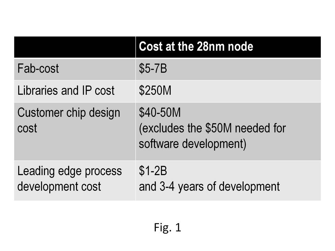
The first set of numbers he quoted is shown in Fig. 1. It shows the cost of development for the 28nm-node. He said the numbers involved are so high that leading edge process nodes make economic sense only for products with high volumes :-( He also mentioned that the 28nm node is going to be a “long-lived” node, not many people will want to scale beyond that…
Hmmm… what do I think of Dirk’s numbers in Fig. 1? Well, I think semiconductor startups are becoming an endangered species… The numbers quoted in Fig. 1 have ensured VCs don’t fund semiconductor startups anymore :-( It costs $100M for a leading edge design, and if you’re a startup, you typically don’t make money off your first product. So, you need to spend $100-150M more on your second product before you can turn a profit. The VC therefore needs to invest $200-250M and wait at least 5 years before he gets any return on investment. On the other hand, in a software startup such as Groupon, you invest $5M and it gets converted to $5B in just 2 years!

Another set of numbers Dirk presented are shown in Fig. 2. You can see the cost of patterning a single litho layer with double patterning is 1.7x higher than for single patterning… EUV can help, said Dirk (as Fig. 2 indicates). But then, EUV seems perennially delayed (see my post from 2 weeks back on the subject here). People are, in fact, thinking of costlier quad patterning approaches for future nodes. The bottom line: Double-patterning and quad-patterning are pretty costly, and make conventional scaling difficult moving forward.
The way to deal with these issues, according to Dirk, is collaboration. He talked about their collaborative process development with IBM and Samsung and also about the collaborative development they’re having with design houses to build products. He said the industry needs to look at EUV and 3D packaging quite seriously to bring cost down.
There were a number of questions I had for Dirk, but I really couldn’t ask them in public since they were kind of sensitive… he had to rush off after the talk, so I couldn’t ask him these questions in a one-on-one conversation either.
- Does it make economic sense to build fabs in the US and Europe? It is well known that the wafer cost is 30-40% lower in Taiwan/Singapore than in the US/Europe due to government concessions and tax breaks. For example, I hear Singapore pays 60% of the equipment costs and products are tax-free for 10 years when one builds a fab there. That’s a lot of cost savings, and that’s what drove manufacturing to the Far-East. Does Globalfoundries plan to have more capacity in Singapore and Abu Dhabi moving forward (at least when compared to the US and Europe)?
- What volumes do you need to turn a profit for a 28nm product (in the year it is introduced)? If you did a plot of volumes required vs. technology node (for different nodes), maybe you can figure out the economic limits of conventional scaling for different applications. For someone with the volumes that AMD has, when is it economically unviable to scale?


 RSS Feed