A few months back, we received an invitation to speak at the AVS 3D workshop in San Jose. We felt it would be a good opportunity to discuss our monolithic 3D DRAM technology, so we accepted the organizers' kind invitation. The workshop happened last week. Overall, it was a fun event to speak at. I was impressed with the questions asked by people in the audience, and also their enthusiasm for the subject. The organizers had planned the event very well and the room was packed to it's capacity (with ~150 people). You can find details of this workshop here. Other speakers at the workshop were Sesh Ramaswami from Applied Materials, Valeriy Sukharev from Mentor Graphics and Robert Rhoades from Entrepix.
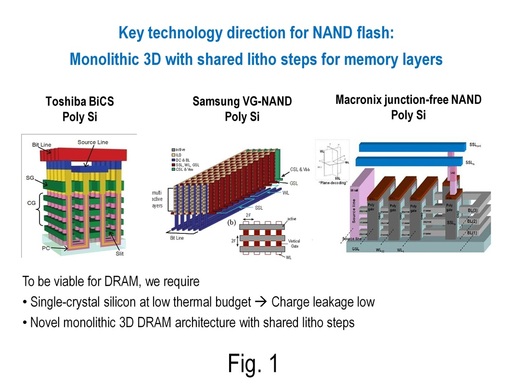
Let's now talk about the technology itself. As many of you know, the industry has been aggressively pursuing monolithic 3D approaches for NAND flash memory wherein litho steps are shared among multiple memory layers (see my old blog-post titled "Looking beyond lithography"). Toshiba has their version called Bit Cost Scalable (BiCS) Technology, while Samsung, Hynix and Intel/Micron have their own approaches. Fig. 1 summarizes these schemes. The common thing with all these approaches is the use of polysilicon for making NAND flash transistors.
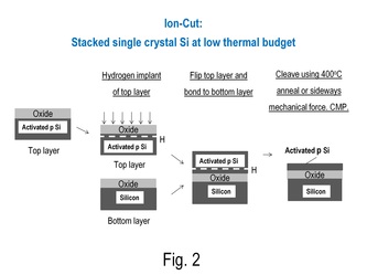
- Stacked single crystal silicon layers produced with low thermal budget
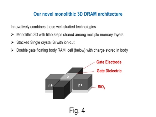
- A novel monolithic 3D DRAM architecture with shared litho steps
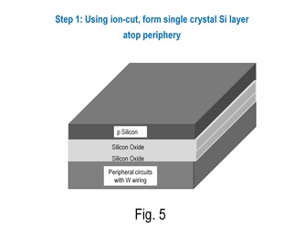
- Step 1: Ion-cut is used to transfer a p-type single crystal silicon layer atop the peripheral circuits of the DRAM as depicted in Fig. 5. Notice how the peripheral circuits are placed under the memory array... this improves the array efficiency and allows smaller-size blocks that offer high performance.
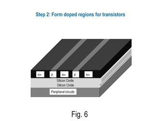
- Step 2: Using litho and implant, n+ doped regions are formed as shown in Fig. 6.
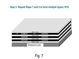
- Step 3: Using steps similar to Step 1 and Step 2, a silicon-silicon dioxide multilayer sandwich is formed as described in Fig. 7. A high temperature anneal is conducted to activate dopands in multiple layers of memory at the same time.
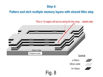
- Step 4: Using the same litho and etch step, multiple layers of memory are defined as shown in Fig. 8.
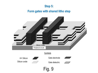
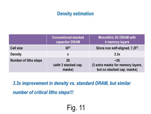
- Step 5: Gates are formed for multiple levels of memory at the same time as described in Fig. 9. Since the source and drain regions are defined in Step 2 and Step 3 and gates are formed separately in Step 5, the process is not self-aligned, which will produce a density penalty of around 20%.
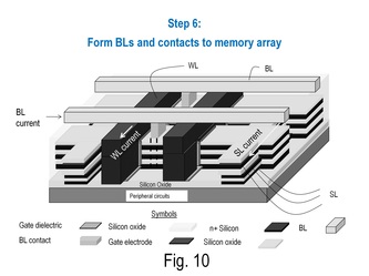
- Step 6: Using another shared litho step, bit-line contacts are formed to multiple levels of memory. Bit-lines are then made. Contacts to multiple levels of memory are defined with shared litho steps using a process described in [Tanaka, et al., Symposium on VLSI Technology, 2007]. Fig. 10 reveals the structure after this step. Using carefully chosen biases to bit-lines (BLs), word-lines (WLs) and source-lines (SLs), each bit in the memory array can be uniquely addressed.
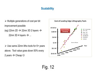
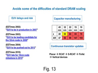
The other key implications of this technology are shown in Fig. 12 and Fig. 13. You'll see that one can get multiple generations of cost per bit improvement without necessarily upgrading the litho tool. For example, a company can do 22nm 2D, then go to 22nm 3D with 2 device layers after two years and then go to 22nm 3D with 4 device layers after another couple of years. So, you'll be able to use the same litho technology for 6+ years and still get cost per bit improvement! Since tools depreciate in value quite significantly every two years, it is a key win. With conventional 2D scaling, one would need to move to a new and costly litho technology every two years. New litho tools such as EUV ones are projected to cost around $100M... one can delay this :-)
Fig. 13 shows companies can avoid some of the difficulties of standard DRAM scaling with this monolithic 3D approach. Please see my previous post titled "The most cut-throat portion of the semiconductor industry" to learn more about the difficulties with standard DRAM scaling.
- One of the biggest challenges to DRAM today is the need for continuous upgrades to litho tools every few years. The next big thing in litho, EUV, has been delayed by many-many years. It was supposed to be in production in 2007, but people now say it's too late for 2015! (see Fig. 13) In the absence of EUV, companies have moved to costly double patterning technologies, and in fact, are within a year of going to quad patterning (for NAND flash). The risk of next-generation litho can be avoided by using monolithic 3D and sticking with the same litho tools for more years.
- DRAM stacked capacitors require aspect ratios of >150:1 and dielectric constants of around 70 in a few years. You'll see projections from the Intl. Technology Roadmap for Semiconductors (ITRS) in Fig. 13. To put these numbers in perspective, 20:1 aspect ratios are considered challenging in most parts of the industry and dielectric constants of around 70 require exotic new high-k materials; well-known high-k dielectrics such as hafnium oxide, aluminum oxide and zirconium oxide will not suffice. The ITRS puts a big portion of the stacked capacitor roadmap in red, which means "no-known-solution". If a company moves to monolithic 3D DRAM, it can potentially avoid these challenges.
- The DRAM industry's roadmap requires a major overhaul of it's cell transistors every generation or two. This challenging problem can potentially be avoided by moving to monolithic 3D DRAMs as well :-) If you stick with the same feature size and just add additional device layers every generation, you may not need to upgrade the transistors for that.
I just showed you an approach to increase DRAM density by 3x or more without increasing the number of critical litho steps. This monolithic 3D DRAM technology can provide several years of continuous cost per bit reduction and reduces the burden we put on next-generation lithography. It also tackles challenges with the stacked capacitor and cell transistor that are inherent to 2D-DRAM scaling. There has been almost no prior work on monolithic 3D with shared litho steps for DRAM, and we've got some pretty fundamental patents allowed by the patent office for this technology. Exciting, isn't it? :-)
To get more details of this technology, please see my presentation at the AVS workshop at the following link.



 RSS Feed