Over the past decade, we've seen a slew of rewritable (RW) memory devices: Phase change memory, resistive RAM and MRAM, just to name a few. What is sorely needed is an architecture that allows these RW devices to be built into chips that compete with NAND flash memory. We'll describe MonolithIC 3D Inc.'s solution to this problem in this blog-post...
Its amazing how many rewritable memory startups Silicon Valley has today... check this list out!
- Ovonyx: Phase-change memory (PCM) startup. Has licensed to Samsung, Micron, Intel, others
- Unity Semiconductor: Resistive RAM (RRAM) startup. Has a partnership with Micron
- Adesto technologies: Resistive RAM startup. Funded by Applied Materials, among others.
- Crossbar: Resistive RAM startup. Funded by Kleiner Perkins.
- 4DS: Resistive RAM startup. Working with Sematech.
- Qs Semiconductor: Resistive RAM startup. Working on SiC memory.
- Nantero: Nanotube RAM startup.
- Grandis: MRAM startup.
- Crocus: MRAM startup.
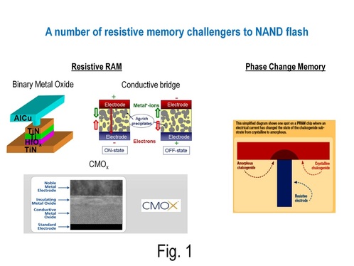
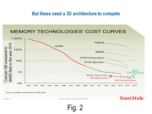
Fig. 2 shows a plot from Dr. Eli Harari, the recently retired SanDisk CEO, that reveals 3D stacking is necessary for all these rewritable memory technologies to compete with NAND flash. This is because the main driver for NAND flash is cost, and without a 3D architecture, its hard to reach costs of NAND flash which is in volume production today, has 3 bits per memory cell and requires just 4 critical lithography steps.
Let's first summarize the 3D architectures that are being explored today by the above startups, and also by bigger companies such as SanDisk, Samsung, Toshiba, Hynix, IBM and others.
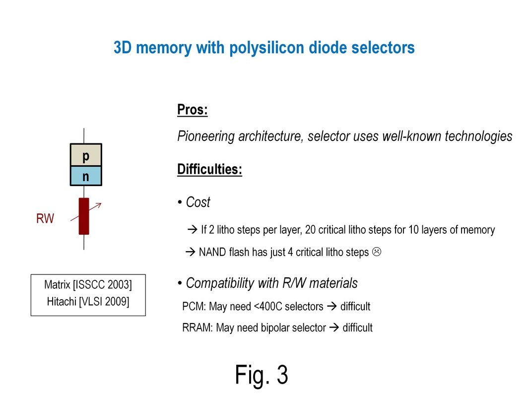
- The most commonly explored architecture is the polysilicon diode selected 3D memory (Fig. 3). This was taken to production by Matrix Semiconductor with antifuse memory in 2003... please see my blog-post on Matrix for more details. While the Matrix architecture is mature and uses well-understood polysilicon diode technology, it has some challenges. One key challenge is cost. The Matrix group revealed in their ISSCC 2003 presentation that they needed 2 litho steps per layer of memory, so for 10 memory layers, they need 20 critical litho steps!! With litho costs sky high nowadays, it is hard to compete with NAND flash which has just 4 critical litho steps :-( Furthermore, while the poly diode selector works well with the antifuses Matrix Semiconductor took to production, it is harder for it to work with rewritable memory elements. PCM compatibility is difficult since the poly diode requires more than 700C process temperatures while PCM melts at 620C. RRAM compatibility is impacted by the fact that the pn junction diode conducts current unidirectionally, while many viable RRAM devices require bidirectional current. To tackle these challenges, companies in the industry took different paths.
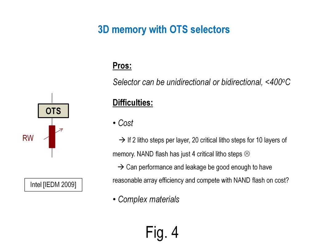
- Intel demonstrated a test-chip in IEDM 2009 that had multiple layers of PCM in series with Ovonic Threshold Switch (OTS) selectors. Please see Fig. 4 for an illustration. The OTS selector could be constructed at less than 400C and it could conduct either unidirectionally or bidirectionally. While this approach tackles the compatibility issue with RW materials such as PCM and RRAM, it still has challenges with litho cost :-( Furthermore, the OTS selector uses complex materials and is harder to process and optimize than a polysilicon diode.
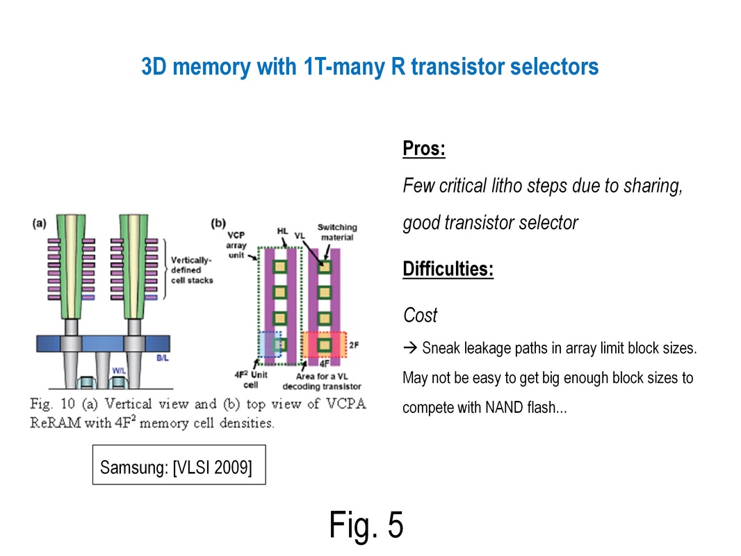
- Samsung showed their approach to 3D resistive memory at the 2009 VLSI Symposium (see Fig. 5). They used shared litho steps to pattern multiple levels of memory at the same time, thereby tackling the litho cost problem. Their use of a transistor selector also allowed compatibility with common RW materials such as PCM and bipolar RRAM. The key challenge with the Samsung architecture is the sharing of a transistor selector among many RW devices. This caused sneak leakage paths which limited block sizes and degraded array efficiency and cost per bit.
Ion-cut, the technology used for manufacturing all SOI wafers nowadays, is one of the key ingredients of this new architecture of ours. It can provide stacked single-crystal silicon at low thermal budgets and is shown in Fig. 7. Ion-cut involves bonding a hydrogen implanted top layer wafer onto a bottom layer wafer, cleaving the bonded stack at it's hydrogen implant plane and later polishing the surface. This process was invented in the early 1990s at CEA -LETI and has been in production since the late 1990s for applications such as SOI wafers.
The other key ingredient of our architecture is the use of junctionless transistors as resistive memory selectors. These transistors rely on using thin silicon channels that are depleted of charge carriers at voltages close to 0V. Macronix has demonstrated NAND flash memory structures made out of junctionless transistors - please see this article for more details. The steps involved in constructing our 3D resistive memory are as follows:
The other key ingredient of our architecture is the use of junctionless transistors as resistive memory selectors. These transistors rely on using thin silicon channels that are depleted of charge carriers at voltages close to 0V. Macronix has demonstrated NAND flash memory structures made out of junctionless transistors - please see this article for more details. The steps involved in constructing our 3D resistive memory are as follows:
- Step 1: Ion-cut is used to transfer a n+ single crystal silicon layer atop the peripheral circuits of the resistive memory as depicted in Fig. 8. Notice how the peripheral circuits are placed under the memory array... this improves the array efficiency and allows smaller-size blocks that offer high performance. Also, the n+ dopants are pre-activated before layer transfer.
- Step 2: Using steps similar to Step 1, a silicon-silicon dioxide multilayer sandwich is formed as described in Fig. 9.
- Step 3: Using the same litho and etch step, multiple layers of memory are defined as shown in Fig. 10.
- Step 4: Gates are formed for multiple levels of memory at the same time as described in Fig. 11.
- Step 5: Using another shared litho step, a via hole is made to multiple levels of memory. A resistive memory element (such as titanium oxide) is deposited following which an electrode is deposited and CMPed (Fig. 12). WL, SL and BL are acronyms for Word Line, Source Line and Bit Line respectively.
- Step 6: Bit-lines are then made. Contacts to multiple levels of memory are defined with shared litho steps using a process described in [Tanaka, et al., Symposium on VLSI Technology, 2007]. Fig. 13 and Fig. 14 reveal the structure after this step. Notice how each memory cell consists of a junctionless transistor in series with a RW memory device. Using carefully chosen biases to bit-lines (BLs), word-lines (WLs) and source-lines (SLs), each bit in the memory array can be uniquely addressed.
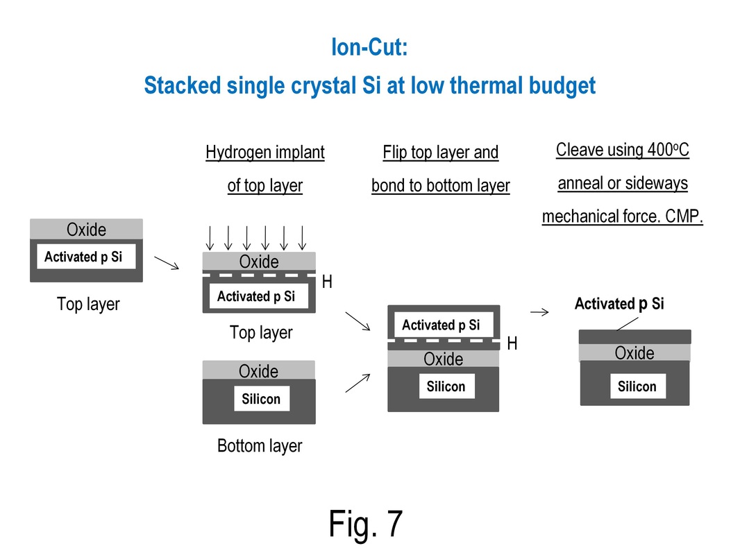
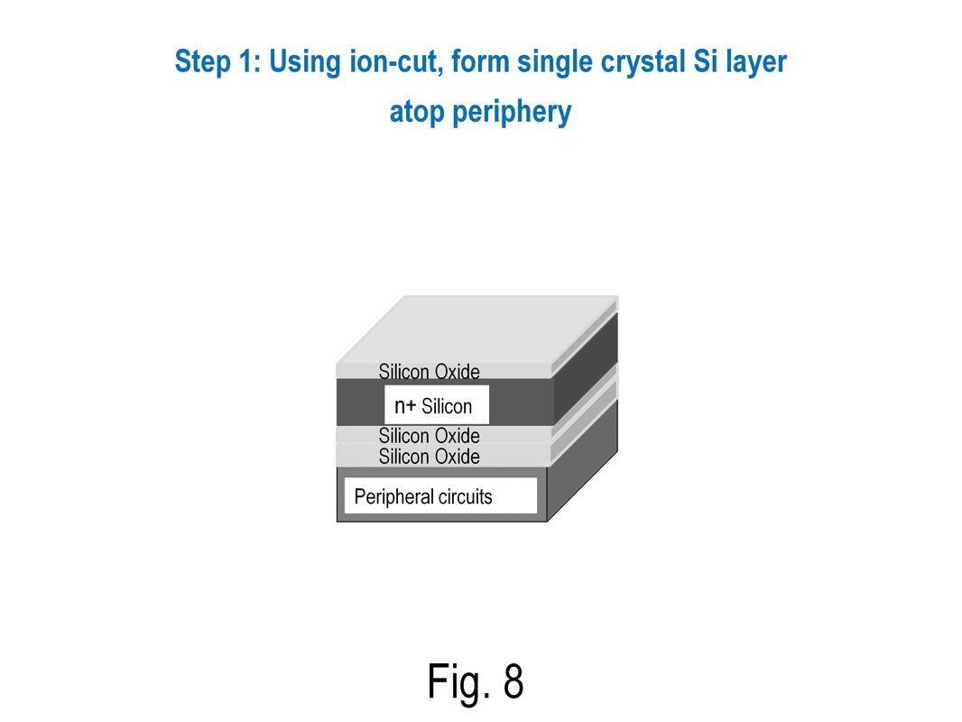
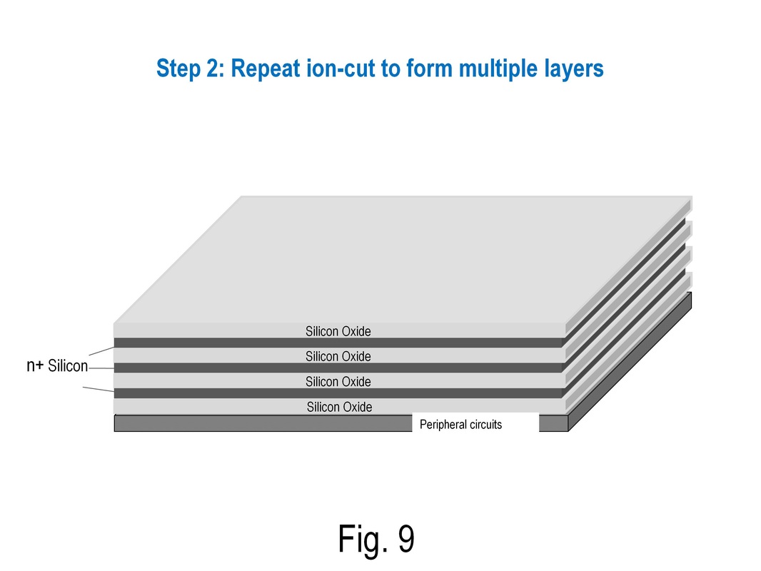

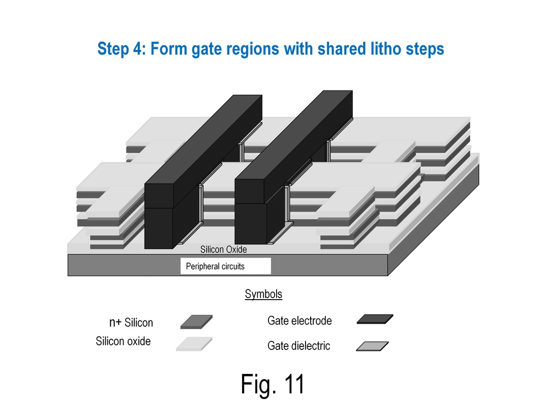
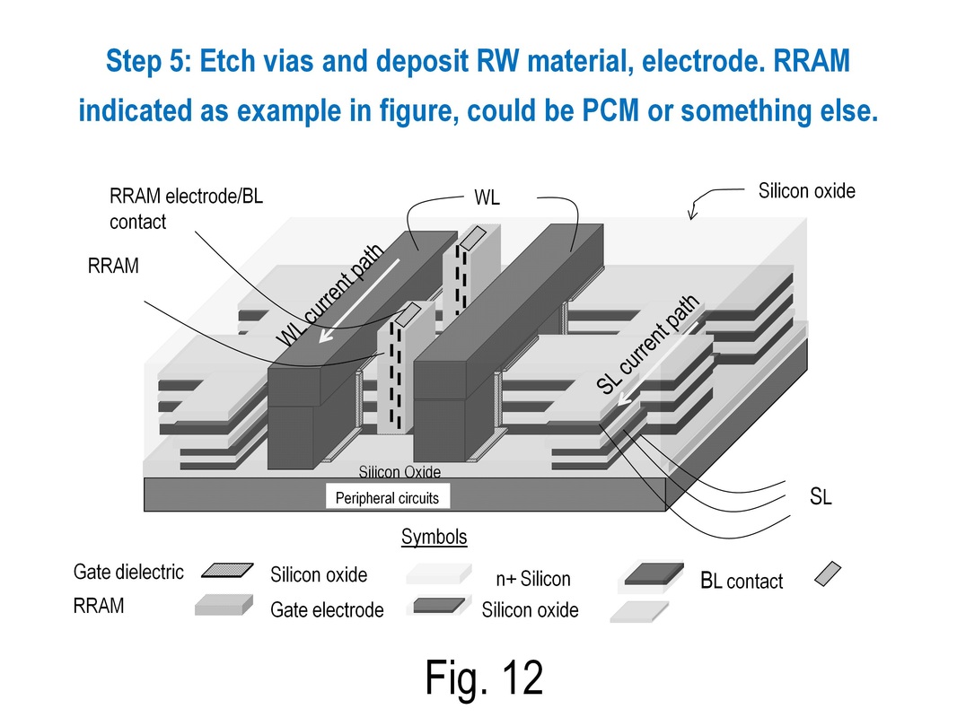
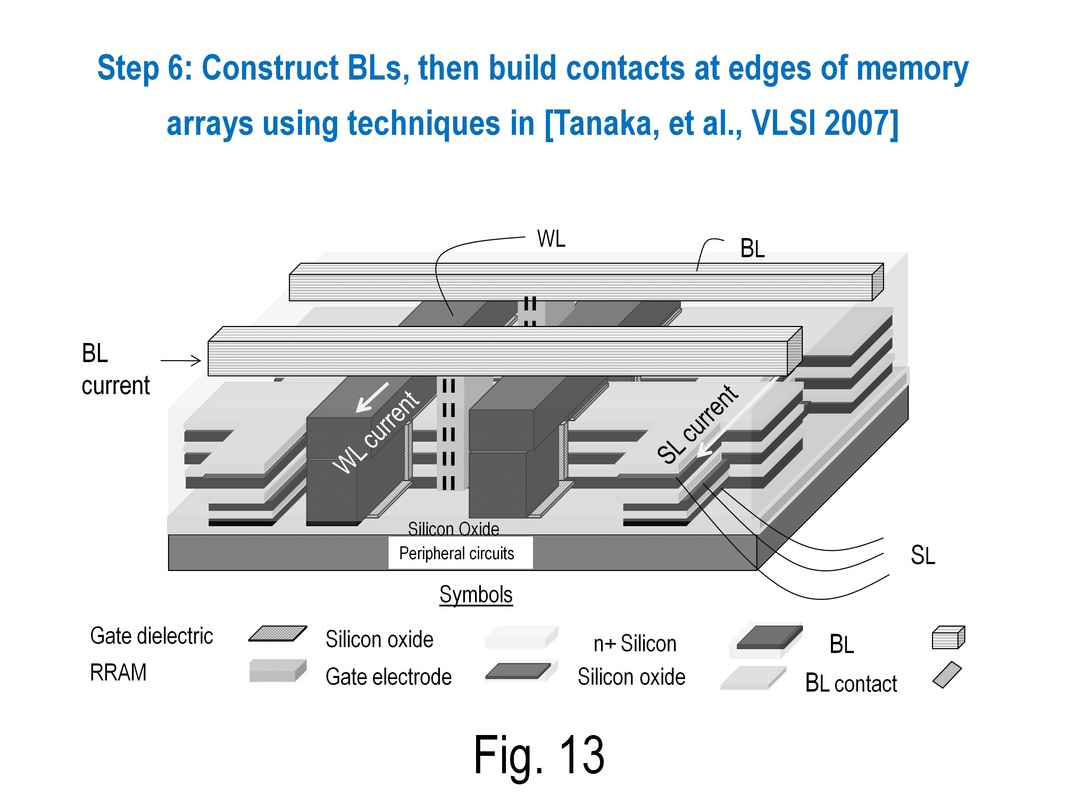

Fig. 15 shows simulation results from Paul Lim for these junctionless devices. It reveals that at the 15nm node, these junctionless transistor selectors can have very small leakage currents (<0.1pA) and can still drive power hungry RW materials. Fig. 16 shows array bias schemes with these selectors... you'll notice leakage currents for unselected cells are negligible, indicating large array sizes and excellent performance are possible. These are key advantages of single crystal silicon transistor selectors.
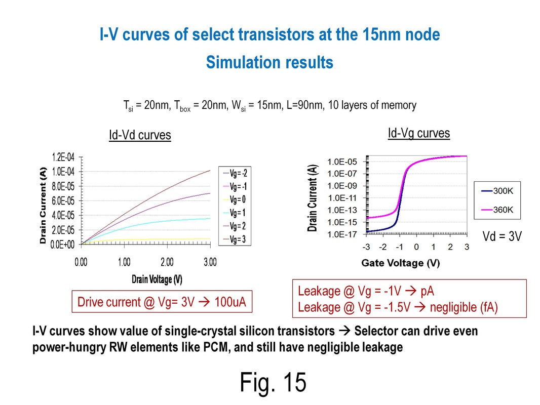
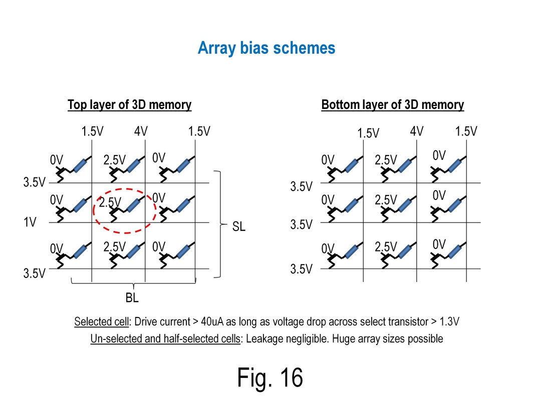
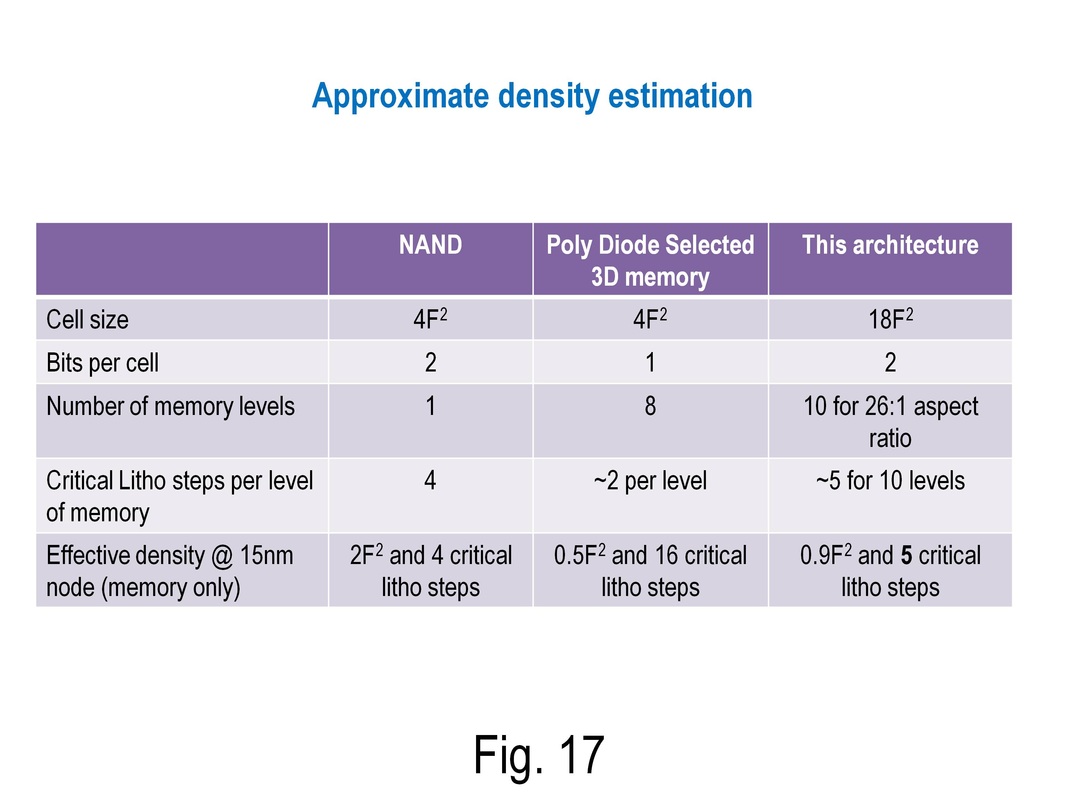
Fig. 17 shows approximate density estimation for our architecture. The architecture has 0.9F(square) cells and ~5 critical litho steps, while a poly diode selected 3D memory requires 16 critical litho steps for 0.5F(square) cells. To put this in perspective, NAND flash has 2F(square) cells and ~4 critical litho steps. As mentioned previously, the large number of litho steps needed for poly diode selected 3D memory are a key challenge both for cost per bit and fab cap-ex. Our new architecture tackles this issue. Fig. 18 reveals other advantages of our architecture over the poly diode selected 3D memory, such as use of a three terminal selector, high performance due to low leakage and high forward current drive of the selector, possibility for bipolar operation and sub-400C construction of the selector.

To summarize,
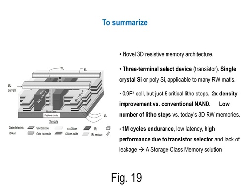
We've described a novel 3D resistive memory architecture in this blog-post (see Fig. 19). It can be useful for many types of rewritable memory materials such as phase change memory and resistive RAM due to its sub-400C process temperatures and use of a three-terminal selector. It offers significant density advantages over NAND flash without incurring an increase in litho cost... this is a key differentiator from other types of 3D RW memories and is enabled by the use of shared litho steps. This architecture could produce an effective storage class memory due to the possibility of getting high endurance and high performance at NAND flash-like densities.
We've described a novel 3D resistive memory architecture in this blog-post (see Fig. 19). It can be useful for many types of rewritable memory materials such as phase change memory and resistive RAM due to its sub-400C process temperatures and use of a three-terminal selector. It offers significant density advantages over NAND flash without incurring an increase in litho cost... this is a key differentiator from other types of 3D RW memories and is enabled by the use of shared litho steps. This architecture could produce an effective storage class memory due to the possibility of getting high endurance and high performance at NAND flash-like densities.


 RSS Feed