
We have a guest contribution from Zvi Or-Bach, the President and CEO of MonolithIC 3D Inc. Mr. Or-Bach discusses about the latest news in semiconductor industry, the headlines that dominated last week's news papers about TSMC and Intel.
On January 14, 2014 we read on the Investors.com headlines page - Intel Seen Gaining Huge Pricing Advantage Over TSMC. Just three days later comes the responding headline: TSMC: We're "Far Superior" to Intel and Samsung as a Partner Fab.
These kinds of headlines are not seen too often in the semiconductor business domain and it is not clear what the objectives are for such. It will be hard to believe that this is an attempt to manipulate the investor community, yet there are only a handful of super high volume design wins that are driving the leading edge devices, and for those wins the fight should be taking place in the 'board' room. So let’s dive a bit into the details behind these headlines.
The first headline relates to Jefferies analyst Mark Lipaci releasing an analysis report stating: "Intel will have a die size and transistor cost advantage over Taiwan Semiconductor (TSM) for the first time by fourth-quarter 2014, which could lead to a 50% pricing advantage in processors in 12 months, and a 66% pricing advantage in 36 months". We can find more information in the blog titled: Intel: Primed for Major Phone, Tablet Share on Cheaper Transistors, Says Jefferies. Quoting Lipaci: "At the same time that Intel has started focusing on computing devices in mobile form factors, it appears that TSMC is hitting a wall on the transistor cost curve. The chart below was presented by TSMC’s CTO. We believe that due to Intel’s larger R&D budget, its recent focus on the mobile/tablet market, and its higher R&D spend relative to TSMC, that it will produce a lower cost transistor than TSMC for the first time ever in 4Q14. We believe Intel extends that cost lead 24 months after than in 2016."
Lipaci then used the following chart to illustrate the build up of Intel advantage vs. TSMC.
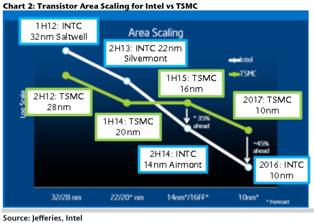
Figure 1
The Jefferies report goes further and provides the following charts for 14nm and 10nm.
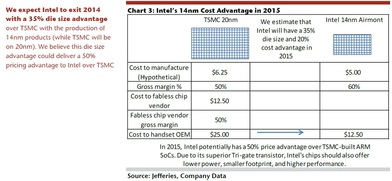
Figure 2
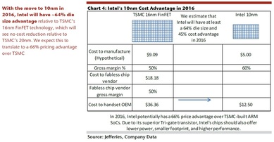
Figure 3
Clearly the primary advantage that the report is pointing out is the lack of the double margin associated with the foundry model vs. the IDM model. It seems that this argument has clearly been disproven by now. In the early days of the foundry industry most IDMs would argue that the foundry model would not work because of the double margin aspect - the foundry would need about 50% gross margin and then the fables company would need an additional 50% gross margin - which would make it completely uncompetitive vs. the IDM. 20 years later it was proven, again, that there is no "free lunch". The chip fabrication business needs a margin to be sustainable and the design business needs a margin to be sustainable. And the better business model is to have those managed by different companies as each could build excellence in its own value proposition. Intel did enjoy for many years effective exclusivity in the Windows based processors. Intel has not been able so far to show much success in mobile or any other non-Windows market. Since Intel is now trying to position themselves as a better foundry than TSMC, then clearly for their potential foundry customers this double margin argument is moot.
The charts above also compare Intel’s cost advantage vs. TSMC older nodes (Intel's 14nm vs. TSMC's 20 nm and Intel's 10nm vs. TSMC's 16nm). It is not clear that Intel is so far ahead. Intel 14nm had been delayed to the first quarter of 2014 and TSMC has committed to be in volume production in the later part of 2014. But the real competition is on the ability to bring fabless companies to volume using one's advanced process node. Key to this is the availability of libraries, EDA full tool set support, and major IP such as ARM processors. It is far from being clear that Intel is really far ahead of TSMC in this critical area. And then, these days it is not so clear that using a more advanced process node buys one an end-device cost advantage. In fact, the foundries have already made it clear that beyond the 28nm node they do not see cost reduction, due to the extra cost associated with advanced node lithography and other issues. Even Intel admitted at their latest analyst day that advanced nodes are associated with escalating depreciation and other costs, as illustrated by the following Intel chart - see the left most graph.
The charts above also compare Intel’s cost advantage vs. TSMC older nodes (Intel's 14nm vs. TSMC's 20 nm and Intel's 10nm vs. TSMC's 16nm). It is not clear that Intel is so far ahead. Intel 14nm had been delayed to the first quarter of 2014 and TSMC has committed to be in volume production in the later part of 2014. But the real competition is on the ability to bring fabless companies to volume using one's advanced process node. Key to this is the availability of libraries, EDA full tool set support, and major IP such as ARM processors. It is far from being clear that Intel is really far ahead of TSMC in this critical area. And then, these days it is not so clear that using a more advanced process node buys one an end-device cost advantage. In fact, the foundries have already made it clear that beyond the 28nm node they do not see cost reduction, due to the extra cost associated with advanced node lithography and other issues. Even Intel admitted at their latest analyst day that advanced nodes are associated with escalating depreciation and other costs, as illustrated by the following Intel chart - see the left most graph.
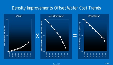
Figure 4
We should note that the Y axes of these graphs are logarithmic which indicate a significant increase of deprecation costs. However, Intel claims it will more than neutralize this increase of costs by accelerating the dimensional scaling when going to 14nm and 10nm, as is presented with the middle graph above. This would lead to an overall sustaining of the historical cost per transistor reduction as is illustrated by the rightmost graph above. Note: the asterisk (*) on those graphs indicates that numbers relating to 14nm and 10nm are forecasts only. Since Intel is committed to be in volume production at the 14nm node any day now, the number associated with 14nm should not be a forecast anymore and we hope to see them released soon.
The simple indication of technology node effective transistor density these days would be the bit cell size. As we have presented many times before, modern SoC device area is dominated by the embedded 6T SRAM. At IEDM 2013, TSMC made public their 6T SRAM bit cell area for 16nm: 0.07 sq. micron. We could not find any Intel public release for their 14nm 6T SRAM bit cell size. We did find an Intel chart for older nodes. This 6T bit cell size chart was presented at IDF2012:
The simple indication of technology node effective transistor density these days would be the bit cell size. As we have presented many times before, modern SoC device area is dominated by the embedded 6T SRAM. At IEDM 2013, TSMC made public their 6T SRAM bit cell area for 16nm: 0.07 sq. micron. We could not find any Intel public release for their 14nm 6T SRAM bit cell size. We did find an Intel chart for older nodes. This 6T bit cell size chart was presented at IDF2012:
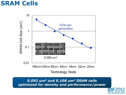
Figure 5
Accordingly the 14nm node 6T SRAM size for conventional dimensional scaling should be 0.092 * (14/22)² = 0.037 sq. micron. And if Intel can really scale more aggressively to compensate for the extra capital costs then their 6T SRAM at 14nm should be about 0.03 sq. micron or even smaller. As we don't have any official number we could wait until their early production devices of the 14nm node get analyzed or to the eventual release of their number. But short of an official number, we did find a 2013 presentation from the TRAMS project, of which Intel is a partner, as illustrated in the following charts:
Figure 6
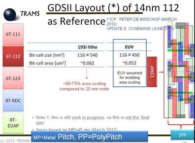
Figure 7
It is now clear that EUV will not be available for the 14nm node, and accordingly the bit cell size from the chart above is 0.062 sq. micron. This is a bit better than that of TSMC but a far cry from 0.03 sq. micron.
If Intel does have a really good number, it would be reasonable to expect that they will make it public soon, to entice the high volume fabless companies such as Qualcomm and Apple to explore Intel’s foundry option.
As for the Jefferies analyst assertion "We believe that due to Intel’s larger R&D budget, its recent focus on the mobile/tablet market, and its higher R&D spend relative to TSMC, that it will produce a lower cost transistor than TSMC", it is not clear if Intel’s R&D budget is truly larger. TSMC’s R&D budget is dedicated to the foundry side of the business while Qualcomm, Apple, ARM and many other fabless vendors R&D budgets support the design part of any new product release. The total ecosystem behind TSMC and ARM is clearly not smaller than that of Intel. In this month’s SEMI ISS Conference, IC Insights provided very interesting numbers regarding the record of 2013 as was reported in a blog titled:Is Intel the Concorde of Semiconductor Companies?
Top 10 CAPEX Spenders in 2013:
- Samsung $12B
- TSMC $11.2B
- Intel $10.5B
- GF $5.5B
- SK Hynix $3.7B
- Micron $3B
- Toshiba $2.9B
- UMC $1.5B
- Infineon $880M
- ASE (OSAT) $770M
Yes, Samsung and TSMC both outspent Intel. Just wait until you see the capacity numbers and you will know why.
Top 10 IC Wafer Capacity Leaders in 2013:
- Samsung 12.6%
- TSMC 10%
- Micron 9.3%
- Toshiba 8%
- SK Hynix 7%
- Intel 6.5%
- ST 3.5%
- UMC 3.5%
- GF 3.3%
- TI 3.0%
Clearly Intel is not larger than TSMC as a foundry and it is not clear why would it have a sustainable per transistor cost advantage.
Cost is important but it is far from being the only parameter when choosing a foundry partner. Selecting a foundry partner is truly selecting a partner. The design of leading edge devices is a very costly and lengthy effort, and has a pivotal effect on the business success for the fabless customer. TSMC had built trustful relationships for many years with its fabless customers. It is not clear how easy it is going to be for Intel to become a trustful foundry partner. So far it seems that Intel is still a proud IDM that insists that its customer will support its branding like the "Intel Inside" campaign or the recent announcement of Branding the cloud: Intel puts its stamp on cloud services across the globe. Intel’s repeating emphasis of their transistor cost advantage vs. that of TSMC suggests that Intel considers TSMC as their main competition for the mobile and tablet business. But then their consistent offering of SoC products for the space, as illustrated by the recent Intel chart below, and the Jefferies' cost analysis above, suggests that Intel is actually an IDM competing with the likes of Qualcomm in this space. It may create concerns in the minds of potential fables customers.
Cost is important but it is far from being the only parameter when choosing a foundry partner. Selecting a foundry partner is truly selecting a partner. The design of leading edge devices is a very costly and lengthy effort, and has a pivotal effect on the business success for the fabless customer. TSMC had built trustful relationships for many years with its fabless customers. It is not clear how easy it is going to be for Intel to become a trustful foundry partner. So far it seems that Intel is still a proud IDM that insists that its customer will support its branding like the "Intel Inside" campaign or the recent announcement of Branding the cloud: Intel puts its stamp on cloud services across the globe. Intel’s repeating emphasis of their transistor cost advantage vs. that of TSMC suggests that Intel considers TSMC as their main competition for the mobile and tablet business. But then their consistent offering of SoC products for the space, as illustrated by the recent Intel chart below, and the Jefferies' cost analysis above, suggests that Intel is actually an IDM competing with the likes of Qualcomm in this space. It may create concerns in the minds of potential fables customers.
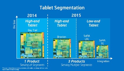
Figure 8
And as a final note, we don't know how much better the Intel process at 14nm and 10nm is vs. that of TSMC. We do know that when we ask someone for directions, if he says ‘make a right turn’ but with his hand he is pointing left, we should go ahead and turn left. So along with all of these confusing statements we learned just this week that Intel Cancels Fab 42, which was supposed to be the most advanced large capacity fab effort of Intel. I wonder if it should be considered as the hand pointing....


 RSS Feed