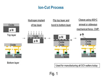
For monolithic 3D, it is often required to form single crystal silicon above copper wiring layers at temperatures lower than 400C. Fig. 1 shows the ion-cut process, which is the most popular method of achieving this objective. Hydrogen is first implanted into a "top layer wafer" to create a defect plane. This "top layer wafer" is then flipped and bonded onto a "bottom layer wafer" having transistors and copper wiring.After this, the structure is cleaved at the defect plane using a 400C anneal or a sideways mechanical force. Finally, a CMP is done to get a good surface.
Cost-of-Ownership Analysis
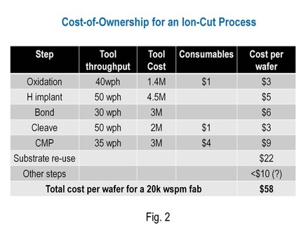
Fig. 2 shows cost calculations for ion-cut using a Sematech Cost-of-Ownership framework. Tool prices and throughputs are obtained from equipment manufacturers who provide tools for these ion-cut process steps. The "top layer wafer" in Fig. 1 is re-used, as is typical in an ion-cut process. The total cost per wafer for a single ion-cut is $58, which is close to estimates that ion-cut practitioners in the industry have provided us. The number seems reasonable... this is what you'd expect of a process that doesn't involve any litho steps. In addition, with passage of time, one would expect throughput of various steps to improve significantly, bringing the price down further.
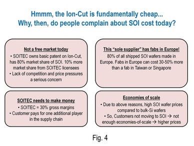
This is because of business issues with SOI wafer manufacturing (see Fig. 4).
- SOI wafer manufacturing is not a free market now: One player, SOITEC, controls 90% of the SOI market today since it owns the basic patent on ion-cut from Michel Bruel. Markets dominated by a single supplier typically have high prices due to lack of competitive pressures.
- This "sole supplier" makes ~80% of its SOI wafers in Europe: Believe it or not, around 80% of SOI wafers are made in Europe today! Its incredibly expensive to have a fab in Europe - that's why all manufacturing is moving to the Far East. A rule of thumb I've heard is that a fab in Taiwan or Singapore is 30-50% cheaper than one in the US or Europe. This is mainly due to government incentives such as tax breaks, lower building costs and lower labor costs. For example, one company I know got a deal from a Far Eastern nation to have a 10 year tax holiday and the government paid 60% of the company's capital expenditure! I also hear SOITEC built its latest fab in Singapore to tackle some of these issues, but that fab only provides only ~20% of its total output now and is running at 10% of its maximum possible capacity. All of us know an under-utilized semiconductor fab is expensive... (Note that some of the numbers in this paragraph are things I heard from industry sources, they are not official estimates)
- Additional player in the supply chain: A company providing SOI wafers today buys a bulk silicon wafer, does the ion-cut process on it and then sells the finished wafer to foundries and IDMs. You're essentially adding an additional player in the supply chain here, with his own margin requirements. Ion-cut manufacturers such as SOITEC have 30% gross margins, so the customer pays extra for this.
- Not enough economies-of-scale: Due to the business constraints listed above, the SOI wafer price overhead is significantly more than the $58 we calculated above. So, SOI adoption has not proceeded as fast as expected, and one cannot reach high enough economies-of-scale. This, in turn, keeps price high compared to bulk Silicon wafers, which hinders adoption. This chicken-and-egg problem (high prices --> low adoption --> not enough economies of scale --> high prices) is a concern.
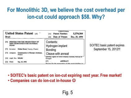
- Many people in the ion-cut community believe the business situation for ion-cut will change on September 15, 2012. Why? Because the basic patent from Bruel describing ion-cut expires that day. Check out patent number 5374564 at the US Patent Office Website. It talks about all the technologies described in Fig. 1: the atomic species implant, bonding, cleaving with anneal, surface cleans, etc. See Fig. 5 for more details. Once the ion-cut becomes a public-domain technology, we believe a free market situation will arise, benefiting everyone. Competition will lower prices which will boost adoption significantly.
- For Monolithic 3D applications, we feel the best way forward is for each company (eg. TSMC, Intel, ST, Toshiba, Fujitsu, Samsung, Micron, etc) to do the ion-cut in-house. So, these companies would place equipment for H implant, bond and cleave in their own fabs and run this process themselves. This will keep costs down since the problems described in Fig. 4 can be avoided, and this will be possible after 2012. One could approach the $58 price per ion-cut that I showed in Fig. 2.
The price per ion-cut could be as low as $58, which is miniscule compared to wafer cost of a logic wafer (~$4000), NAND flash memory wafer (~$1500) or DRAM wafer (~$2000). This is encouraging for the monolithic 3D application, since ion-cut is the most popular technique to get stacked single crystal silicon layers. Once these stacked single crystal silicon layers are obtained, one can use MonolithIC 3D Inc.'s innovative device architectures to build high-quality 3D chips.



 RSS Feed