We have a blog-post today from Paul Lim, Monolithic 3D Inc.'s Principal Device Engineer. Paul is an ex-Stanford grad and is a visiting researcher at Stanford University's Center for Integrated Systems... he will talk about 3D-IC work going on at Stanford.
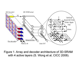
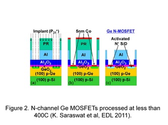
The main research work on 3D integrated circuits nowadays at Stanford University is under a DARPA sponsored grant headed by Professor Simon Wong and involves a total of 10 professors. In Professor Simon Wong’s own group, the main focus so far is on 3D circuits, such as a 3D SRAM architecture (Figure 1). Part of the research is on fabricating Germanium on Insulator (GeOI) MOSFETs, which are promising for 3D-IC’s owing to their lower process temperatures. In this area, Prof. Jim Plummer and Prof. Krishna Saraswat took the lead. Prof. Saraswat's team recently demonstrated Germanium MOSFETs fabricated at less than 400C using metal induced dopant activation (Figure 2).
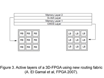
The group of Professor Abbas El-Gamal worked on 3-D FPGA’s by stacking two configuration memory layers and a switch layer on top of a standard CMOS layer, and then using a new routing fabric (Figure 3). They show that a 3D-FPGA using this fabric can achieve a 3.3x improvement in logic density, a 2.35x improvement in delay, and a 2.82x improvement in dynamic power consumption over the same baseline 2D-FPGA. Professor El-Gamal is already well-known in the signal processing field and yet he shows his wide expertise by dabbling in 3D-IC’s as well.
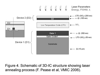
Outside of the DARPA project, various Stanford professors are involved in 3D-IC research in one form or another. One of these is Professor Fabian Pease, called out of retirement due to his continuing value to the Stanford semiconductor community. His group worked on laser annealing techniques to achieve dopant activation, and low temperature deposition processes like LPCVD for forming the gate dielectrics in the upper levels of 3D IC’s (Figure 4). Calculations and experiments indicate that using these process techniques together maintains the quality and reliability of circuits at lower levels. As a side note, Ultratech pioneered the laser spike anneal technology, which it claims as the only viable solution to enable the continuation of Moore's Law for advanced nodes. Real serious stuff. No wonder their employees all wear suits to work everyday! Professor Pease is a man of many interests, and other than 3D-IC’s, his research over the years covered Electron Beam Lithography, Negative Electron Affinity Photocathodes, and various novel transistor structures. Interestingly, he was also the first to investigate the thermal management of chips using microchannels 30 years ago, way back in 1981.
Talking about thermal management in chips, it is obviously a bigger problem in 3D-ICs. At Stanford University, Professor Kenneth Goodson in the Mechanical Engineering Department showed one can tackle this problem by integrating a micro-channel network in 3D IC’s driven by cooling fluids. His theoretical calculations indicate that a layer of integrated micro-channel cooling can remove heat densities up to 135 W/sq. cm within a 3D architecture with a maximum circuit temperature of 85°C. Professor Goodson also happens to be a classically trained professional opera singer, and he still gives performances every once in a while.
So it looks like Stanford University, with its cast of superstar professors, is well-positioned to lead the innovation yet again, this time in the field of 3D-ICs!


 RSS Feed