When I discuss 3D-ICs with people, they almost always bring up heat removal and power delivery, and ask me how to deal with these issues. Let's address the power delivery issue with this blog-post...

Why is power delivery an issue for 3D-ICs?
Let's consider the 3D-IC simulation shown on our webpage (link). For a 22nm 600MHz logic core,
2D implementation: 1.6W, 0.8V, 2A, 50 sq. mm --> 4 A/sq. cm
Monolithic 3D implementation: 0.8W, 0.8V, 1A, 12 sq. mm --> 8 A/sq. cm
You can see that the current density for 3D-ICs is higher... As many of you know, delivering power with low-losses through the resistive and inductive parasitics of the chip, package and board is difficult even for 2D-ICs. For 3D-ICs, it could be more of a challenge :-( To enjoy the large benefits offered by 3D, we need to find good ways of handling power delivery...
Here is our toolkit for tackling the 3D power delivery problem:
- Throw cost at the problem: The simplest solution is to throw cost at the problem, and add additional resources, such as decoupling capacitance, vias, I/Os or routing area, to the power distribution network. My Georgia Tech office-mate and good friend, Gang Huang, explored these trade-offs with his 2007 EPEP paper... it was one of the first papers on 3D power delivery and has been referenced by quite a few people (link to paper).
- CAD tools that optimize power density: A number of CAD tools have been developed for 3D-ICs that floorplan and place blocks/cells such that total wire length is minimized while keeping temperature <85C. These CAD tools make sure one doesn't place two power-hungry blocks/cells atop each other. While most of this work was done to address heat removal issues, it could also tackle the power delivery problem...
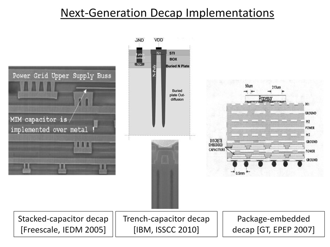
- Next-generation decaps: Alternatives to gate-oxide decaps have been developed in the past few years, and are shown in the above figure. Freescale used stacked capacitor decaps in products and showed ~10% improvement in clock frequency. IBM has e-DRAM integrated with logic in their latest process technologies, and uses trench capacitors for decoupling. They claim 20x less area vs. standard gate-oxide decaps. A friend of mine tells me IBM is offering e-DRAM and trench decaps as a standard option for their foundry process, and this has encouraged adoption of trench decaps among their customers. The academic world has some interesting decap implementations too... Back in my grad school days, the Georgia Tech Packaging Research Center had a program to embed decaps in packages. If package-level decaps were placed with low inductance between them and the chip, they were found to reduce the amount of on-chip decoupling required (link).
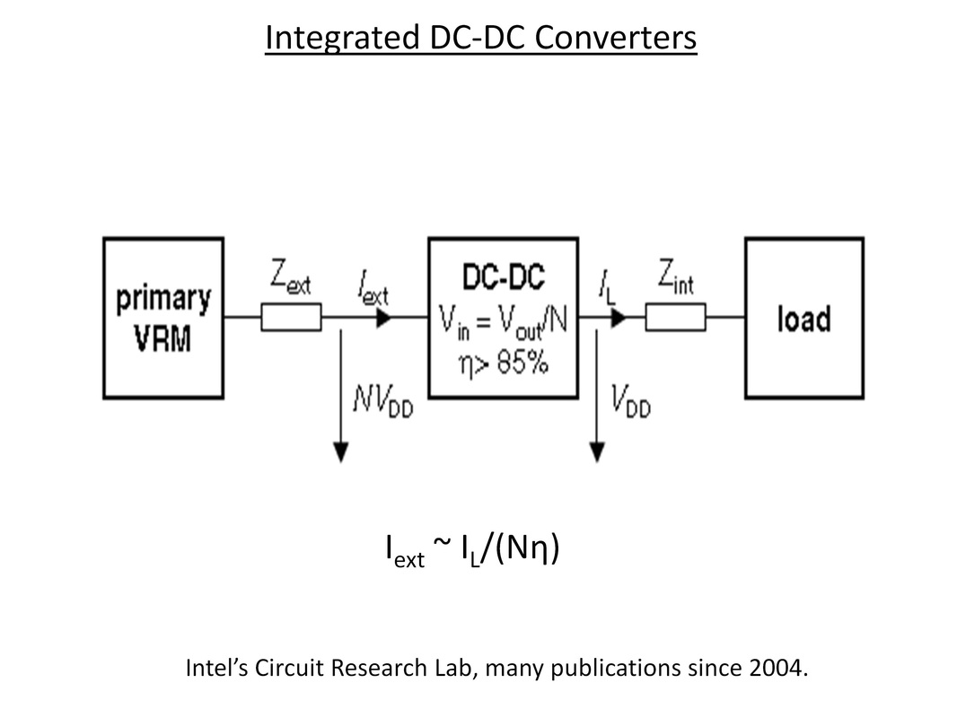
- Integrated DC-DC converters: Intel's Circuits Research Lab has a program to develop integrated DC-DC converters. The basic idea is to deliver voltage to a chip at 2V, then use an on-chip DC-DC converter to convert it to 1V (for example). Please see the figure above. What's the benefit of this? If you have to deliver 100W @ 2V, the current passing through the package and the board is 100W/2V = 50A instead of 100W/1V = 100A. Losses in the power delivery path are reduced significantly if lower currents need to be delivered. Not just that, future chips are expected to have 10s to 100s of logic cores and SRAM blocks, each running at its own optimized voltage to save power. On-chip DC-DC converters enable simple and cost-effective implementation of multiple power supplies. The key challenge to effective implementation is the requirement for high-quality on-chip inductors - it often requires new materials and process steps.
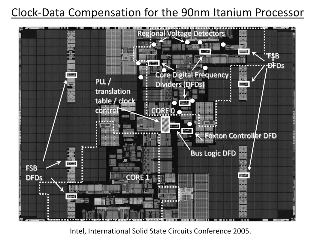
- Clock-data compensation: This was a scheme first used in the Itanium Montecito processor, please see the above figure. The idea involves having circuits (called Regional Voltage Detectors) at various locations on the chip to figure out the amount of supply noise. Once the supply noise extent is found, the clock is adjusted at these locations with Digital Frequency Dividers such that the clock path sees similar speed-up or slow-down as the data path. This "clock-data compensation" can reduce the margin needed for supply noise dramatically, and is relevant since a big part of supply noise is low-frequency (<100MHz). "Clock-data compensation" is somewhat complicated to implement for a single core or dual core chip due to synchronization issues between clock domains, but in the future, when we have 10s of cores all running at their own frequency, it should be easier to implement.
- Microarchitectural di/dt control: Ed Grochowski and his colleagues at Intel wrote two good papers on this topic in 2002 (Check out Ed Grochowski's website here, its quite nice and interesting). Please see the figure above, which shows the simulated chip voltage for some benchmark software. You'll notice that the worst case noise is encountered only for a short period of time. By using this "worst-case margin" for all cases, we increase supply voltage and power consumption significantly. Grochowski, et al. figured out ways of estimating supply voltage based on instructions being run by the processor, and turned off blocks when the supply voltage was going to droop too much. Note that a lot of the supply noise is at <100MHz, so it can be controlled using feedback circuits in a processor run at >3GHz. The authors estimated that the performance penalty of this scheme was small since the worst-case condition happened infrequently.
We've seen in this blog-post that there are many ways of handling the power delivery issue for 3D-ICs. An architect could pick one or more of these techniques based on his or her trade-off analysis and risk profile. It looks like power delivery will not be a show-stopper to 3D-ICs, but will require good engineering, especially for chips that need >20W. Of course, the first logic-on-logic 3D-ICs will probably consume <1W and be used for smart-phones and tablets. It should be easier to handle the power delivery problem there.
- Post by Deepak Sekar


 RSS Feed