
We have a guest contribution today from Paul Lim, MonolithIC 3D Inc.'s Principal Device Engineer. Paul is one of the best device simulation people I know, and has spent many years working on that subject. He talks about how device simulations can aid 3D-IC research.
A long long time ago, people thought they understood most of the details of the workings of semiconductor devices. Life was simple – diodes were wide-based, and MOSFETs had long channels. In the world of multi-micron channel lengths, models involving abrupt junctions and rectangular depletion regions were enough. All you had to do was plug these simple models into Poisson’s equation, couple it with the electron and/or hole continuity equation, add a transport equation, and viola, a simple closed-from analytical solution pops out. Now whatever you wanted to know about current outputs with certain voltage inputs are easily determined by simple plug-and-play. For diodes, it was easy enough to just use the equations so painstakingly derived by Shockley. Unlike in process modeling, where the equations are empirical in nature and necessarily complicated, the closed-form analytical solutions in device modeling are simple, and yet matched well with experimental results so there was no need for numerical simulations on computers.
But then in the early 80’s some people realized that this comfortable life is not going to last forever. As how it usually happens in these things, a select group of university professors, who typically think 10 years ahead, began to see that future devices will have junctions that are not as abrupt, channel inversion layers that are not just a simple sheet of charge, and insulators that are not leak-proof. They realized that this is going to be a big problem, as the simple analytical equations derived from the simple models will not be very accurate anymore compared to the experimental data. To no surprise, these professors are from Stanford University, where it is claimed that Silicon Valley was fathered. Professor Robert Dutton and his TCAD group, together with Professor James Plummer, led the work on creating simulation tools for semiconductor device and process modeling. This project gave birth to the development of the Pisces device simulator and the Suprem process simulator. Eventually, these simulators became the core of the simulation packages that companies like Synopsys and Silvaco used for their commercial semiconductor simulators. As a side note, Professor Dutton got his BS, MS, and PhD degrees from UC Berkeley, and despite being currently a Stanford Professor, would still cheer in the annual football Big Game between the two rival schools on the side of the Golden Bears.
Nowadays, any advanced device research is inconceivable without the help of device simulators. Devices now are just too complex and too small to involve only simple calculations. For instance, feature sizes of a few nanometers require the use of quantum mechanics in understanding the device behavior. At this level, the high complexity and nonlinearity of the equations make analytical solutions impossible. Also, the cost of manufacturing prototypes of these complex devices have gone up by orders of magnitude. It is simply much easier and cheaper to let the device design be tested and optimized by the simulators, especially in the beginning.
In the new field of 3D-ICs, process limitations will require the use of unconventional device structures like for instance, recessed channel transistors and gated resistors. These either have more complicated structures or involve more complicated physics, and the proper simulation of their behaviors requires the inclusion of numerous physical models. A researcher in the field therefore, must necessarily be knowledgeable in the intricacies of device physics like various carrier-carrier scattering models, transport phenomena, and tunneling mechanisms to determine which ones are relevant and make sure that they are compatible with the use of each other.
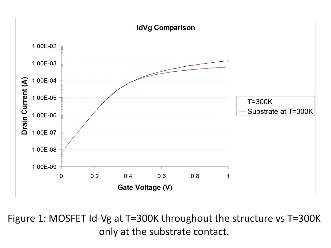
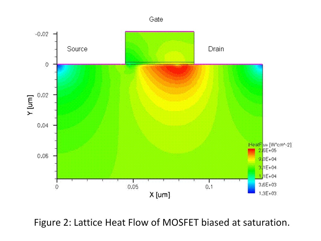
Very few researchers who use device simulators even realize that the simulators can also be used to include thermal effects. This is accomplished by the simple coupling of the heat equation to the usual Poisson, continuity and transport equations. On the issue of heat dissipation in 3D-ICs, this turns out to be useful in the analysis of thermal generation in devices and the design of thermal pathways for dissipation.
But then in the early 80’s some people realized that this comfortable life is not going to last forever. As how it usually happens in these things, a select group of university professors, who typically think 10 years ahead, began to see that future devices will have junctions that are not as abrupt, channel inversion layers that are not just a simple sheet of charge, and insulators that are not leak-proof. They realized that this is going to be a big problem, as the simple analytical equations derived from the simple models will not be very accurate anymore compared to the experimental data. To no surprise, these professors are from Stanford University, where it is claimed that Silicon Valley was fathered. Professor Robert Dutton and his TCAD group, together with Professor James Plummer, led the work on creating simulation tools for semiconductor device and process modeling. This project gave birth to the development of the Pisces device simulator and the Suprem process simulator. Eventually, these simulators became the core of the simulation packages that companies like Synopsys and Silvaco used for their commercial semiconductor simulators. As a side note, Professor Dutton got his BS, MS, and PhD degrees from UC Berkeley, and despite being currently a Stanford Professor, would still cheer in the annual football Big Game between the two rival schools on the side of the Golden Bears.
Nowadays, any advanced device research is inconceivable without the help of device simulators. Devices now are just too complex and too small to involve only simple calculations. For instance, feature sizes of a few nanometers require the use of quantum mechanics in understanding the device behavior. At this level, the high complexity and nonlinearity of the equations make analytical solutions impossible. Also, the cost of manufacturing prototypes of these complex devices have gone up by orders of magnitude. It is simply much easier and cheaper to let the device design be tested and optimized by the simulators, especially in the beginning.
In the new field of 3D-ICs, process limitations will require the use of unconventional device structures like for instance, recessed channel transistors and gated resistors. These either have more complicated structures or involve more complicated physics, and the proper simulation of their behaviors requires the inclusion of numerous physical models. A researcher in the field therefore, must necessarily be knowledgeable in the intricacies of device physics like various carrier-carrier scattering models, transport phenomena, and tunneling mechanisms to determine which ones are relevant and make sure that they are compatible with the use of each other.
Very few researchers who use device simulators even realize that the simulators can also be used to include thermal effects. This is accomplished by the simple coupling of the heat equation to the usual Poisson, continuity and transport equations. On the issue of heat dissipation in 3D-ICs, this turns out to be useful in the analysis of thermal generation in devices and the design of thermal pathways for dissipation.
3D-IC layer transfer techniques involving several materials of various coefficients of thermal expansion or lattice constants may introduce strain into the structures, thus potentially affecting carrier mobilities. These kind of effects are also among the modeling capabilities of device simulators, and provide useful feedback on material compatibility.
As we can clearly see, the use of device simulations is enabling innovations in 3D-IC research!
As we can clearly see, the use of device simulations is enabling innovations in 3D-IC research!


 RSS Feed